R526 PENTIUM PCI/ISA MTI-526 Motherboard Settings and Configuration
M TECHNOLOGY, INC.
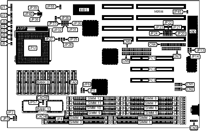
R526 PENTIUM PCI/ISA MTI-526
Processor | CX M1/Pentium |
Processor Speed | 75/80/90/100/120/133/150/166MHz |
Chip Set | SIS |
Video Chip Set | None |
Maximum Onboard Memory | 512MB (EDO supported) |
Maximum Video Memory | 1MB |
Cache | 256/512/1024KB |
BIOS | Award |
Dimensions | 330mm x 220mm |
I/O Options | 32-bit PCI slots (3), floppy drive interface, green PC connector, IDE interfaces (2), parallel port, PS/2 mouse interface, serial ports (2) |
NPU Options | None |
CONNECTIONS | |||
Purpose | Location | Purpose | Location |
Serial port 2 | CN1 | Speaker | J2 |
Serial port 1 | CN2 | Turbo switch | J3 |
PS/2 mouse interface | CN3 | Turbo LED | J4 |
Floppy drive interface | CN4 | Reset switch | J5 |
IDE interface 2 | CN5 | Green PC connector | J6 |
IDE interface 1 | CN6 | IDE interface LED 1 | J7 |
Parallel port | CN7 | IDE interface LED 2 | J8 |
Power LED & keylock | J1 | 32-bit PCI slots | PC1 - PC3 |
USER CONFIGURABLE SETTINGS | |||
Function | Label | Position | |
» | Pipeline address disabled | JP32 | Pins 1 & 2 closed |
Pipeline address enabled (only if burst cache is installed) | JP32 | Pins 2 & 3 closed | |
» | Cache type select write back | JP33 | Pins 1 & 2 closed |
Cache type select write through | JP33 | Pins 2 & 3 closed | |
» | CMOS memory normal operation | JP36 | Pins 1 & 2 closed |
CMOS memory clear | JP36 | Pins 2 & 3 closed | |
Monitor type select CGA | JP45 | Closed | |
Monitor type select EGA/VGA/monochrome | JP45 | Open | |
» | Flash BIOS mode select normal operation | JP55 | Pins 2 & 3 closed |
Flash BIOS mode select programming mode | JP55 | Pins 1 & 2 closed | |
DRAM CONFIGURATION 1 | ||
Size | Bank 0 | Bank 1 |
4MB | (4) 1M x 9 | None |
4MB | None | (1) 1M x 36 |
16MB | (4) 4M x 9 | None |
16MB | None | (1) 4M x 36 |
32MB | (4) 16M x 9 | None |
32MB | None | (1) 16M x 36 |
Note: Bank 0 = SIMM 5, 6, 7 & 8. Bank 1 = SIMM 1 or 2. Board accepts EDO memory. Board also accepts x 32 SIMMS. | ||
DRAM CONFIGURATION 2 | |||
Size | Bank 0 | Bank 1 | Bank 2 |
24MB | (2) 1M x 36 | (2) 1M x 36 | (8) 1M x 9 |
32MB | (2) 2M x 36 | (2) 1M x 36 | (8) 1M x 9 |
48MB | (2) 1M x 36 | (2) 1M x 36 | (8) 4M x 9 |
48MB | (2) 4M x 36 | (2) 1M x 36 | (8) 1M x 9 |
56MB | (2) 2M x 36 | (2) 1M x 36 | (8) 4M x 9 |
72MB | (2) 4M x 36 | (2) 1M x 36 | (8) 4M x 9 |
80MB | (2) 8M x 36 | (2) 1M x 36 | (8) 1M x 9 |
80MB | (2) 1M x 36 | (2) 8M x 36 | (8) 1M x 9 |
88MB | (2) 2M x 36 | (2) 8M x 36 | (8) 1M x 9 |
104MB | (2) 8M x 36 | (2) 1M x 36 | (8) 4M x 9 |
104MB | (2) 1M x 36 | (2) 8M x 36 | (8) 4M x 9 |
104MB | (2) 4M x 36 | (2) 8M x 36 | (8) 1M x 9 |
112MB | (2) 2M x 36 | (2) 8M x 36 | (8) 4M x 9 |
128MB | (2) 4M x 36 | (2) 8M x 36 | (8) 4M x 9 |
136MB | (2) 8M x 36 | (2) 8M x 36 | (8) 1M x 9 |
144MB | (2) 1M x 36 | (2) 1M x 36 | (8) 16M x 9 |
144MB | (2) 16M x 36 | (2) 1M x 36 | (8) 1M x 9 |
144MB | (2) 1M x 36 | (2) 16M x 36 | (8) 1M x 9 |
152MB | (2) 2M x 36 | (2) 1M x 36 | (8) 16M x 9 |
152MB | (2) 2M x 36 | (2) 16M x 36 | (8) 1M x 9 |
DRAM CONFIGURATION 2 (CON’T) | |||
Size | Bank 0 | Bank 1 | Bank 2 |
160MB | (2) 8M x 36 | (2) 8M x 36 | (8) 4M x 9 |
168MB | (2) 4M x 36 | (2) 1M x 36 | (8) 16M x 9 |
168MB | (2) 16M x 36 | (2) 1M x 36 | (8) 4M x 9 |
168MB | (2) 1M x 36 | (2) 16M x 36 | (8) 4M x 9 |
168MB | (2) 4M x 36 | (2) 16M x 36 | (8) 1M x 9 |
176MB | (2) 2M x 36 | (2) 16M x 36 | (8) 4M x 9 |
192MB | (2) 4M x 36 | (2) 16M x 36 | (8) 4M x 9 |
200MB | (2) 8M x 36 | (2) 1M x 36 | (8) 16M x 9 |
200MB | (2) 1M x 36 | (2) 8M x 36 | (8) 16M x 9 |
200MB | (2) 8M x 36 | (2) 16M x 36 | (8) 1M x 9 |
200MB | (2) 16M x 36 | (2) 8M x 36 | (8) 1M x 9 |
208MB | (2) 2M x 36 | (2) 8M x 36 | (8) 16M x 9 |
224MB | (2) 4M x 36 | (2) 8M x 36 | (8) 16M x 9 |
224MB | (2) 8M x 36 | (2) 16M x 36 | (8) 4M x 9 |
224MB | (2) 16M x 36 | (2) 8M x 36 | (8) 4M x 9 |
256MB | (2) 8M x 36 | (2) 8M x 36 | (8) 16M x 9 |
264MB | (2) 16M x 36 | (2) 1M x 36 | (8) 16M x 9 |
264MB | (2) 1M x 36 | (2) 16M x 36 | (8) 16M x 9 |
264MB | (2) 16M x 36 | (2) 16M x 36 | (8) 1M x 9 |
272MB | (2) 2M x 36 | (2) 16M x 36 | (8) 16M x 9 |
272MB | (2) 32M x 36 | (2) 1M x 36 | (8) 1M x 9 |
272MB | (2) 1M x 36 | (2) 32M x 36 | (8) 1M x 9 |
280MB | (2) 2M x 36 | (2) 32M x 36 | (8) 1M x 9 |
288MB | (2) 4M x 36 | (2) 16M x 36 | (8) 16M x 9 |
288MB | (2) 16M x 36 | (2) 16M x 36 | (8) 4M x 9 |
296MB | (2) 32M x 36 | (2) 1M x 36 | (8) 4M x 9 |
296MB | (2) 1M x 36 | (2) 32M x 36 | (8) 4M x 9 |
296MB | (2) 4M x 36 | (2) 32M x 36 | (8) 1M x 9 |
304MB | (2) 2M x 36 | (2) 32M x 36 | (8) 4M x 9 |
320MB | (2) 8M x 36 | (2) 16M x 36 | (8) 16M x 9 |
320MB | (2) 16M x 36 | (2) 8M x 36 | (8) 16M x 9 |
320MB | (2) 4M x 36 | (2) 32M x 36 | (8) 4M x 9 |
328MB | (2) 8M x 36 | (2) 32M x 36 | (8) 1M x 9 |
328MB | (2) 32M x 36 | (2) 8M x 36 | (8) 1M x 9 |
352MB | (2) 8M x 36 | (2) 32M x 36 | (8) 4M x 9 |
352MB | (2) 32M x 36 | (2) 8M x 36 | (8) 4M x 9 |
384MB | (2) 16M x 36 | (2) 16M x 36 | (8) 16M x 9 |
392MB | (2) 32M x 36 | (2) 1M x 36 | (8) 16M x 9 |
392MB | (2) 1M x 36 | (2) 32M x 36 | (8) 16M x 9 |
392MB | (2) 16M x 36 | (2) 32M x 36 | (8) 1M x 9 |
392MB | (2) 32M x 36 | (2) 16M x 36 | (8) 1M x 9 |
400MB | (2) 2M x 36 | (2) 32M x 36 | (8) 16M x 9 |
416MB | (2) 4M x 36 | (2) 32M x 36 | (8) 16M x 9 |
DRAM CONFIGURATION 2 (CON’T) | |||
Size | Bank 0 | Bank 1 | Bank 2 |
416MB | (2) 16M x 36 | (2) 32M x 36 | (8) 4M x 9 |
416MB | (2) 32M x 36 | (2) 16M x 36 | (8) 4M x 9 |
448MB | (2) 8M x 36 | (2) 32M x 36 | (8) 16M x 9 |
448MB | (2) 32M x 36 | (2) 8M x 36 | (8) 16M x 9 |
512MB | (2) 16M x 36 | (2) 32M x 36 | (8) 16M x 9 |
512MB | (2) 32M x 36 | (2) 16M x 36 | (8) 16M x 9 |
Note: Bank 0 = SIMM 1 & 2. Bank 1 = SIMM 3 & 4. Bank 2 = SIMM 5 - 12. Board accepts EDO memory. Board also accepts x 32 SIMMS. | |||
DRAM CONFIGURATION 3 | ||
Size | Bank 0 | Bank 1 |
8MB | (4) 1M x 9 | (1) 1M x 36 |
32MB | (4) 4M x 9 | (1) 4M x 36 |
128MB | (4) 16M x 9 | (1) 8M x 36 |
Note: Bank 0 = SIMM 5 - 8. Bank 1 = SIMM 2. Board accepts EDO memory. Board also accepts x 32 SIMMS. | ||
DRAM CONFIGURATION 4 | ||
Size | Bank 0 | Bank 1 |
8MB | (4) 1M x 9 | (1) 1M x 36 |
32MB | (4) 4M x 9 | (1) 4M x 36 |
128MB | (4) 16M x 9 | (1) 8M x 36 |
Note: Bank 0 = SIMM 9 - 12. Bank 1 = SIMM 1. Board accepts EDO memory. Board also accepts x 32 SIMMS. | ||
DRAM JUMPER CONFIGURATION | |
Configuration | JP4 |
1 | Pins 1 & 2 closed |
2 | Pins 1 & 2 closed |
3 | Pins 2 & 3 closed |
4 | Pins 2 & 3 closed |
CACHE CONFIGURATION | |||
Size | Bank 0 | Bank 1 | TAG |
256KB (A) | (8) 32K x 8 | None | (1) 8K/16K/32K x 8 |
256KB (B) | None | (2) 32K x 32 | (1) 8K/16K/32K x 8 |
512KB | (8) 64K x 8 | None | (1) 16K/32K x 8 |
1MB | (8) 128K x 8 | None | (1) 32K x 8 |
Note: Board will be installed with either standard or burst cache. Both types will not be present. | |||
CACHE JUMPER CONFIGURATION | ||
Size | JP5 | JP6 |
256KB (A) | Pins 1 & 2 closed | Pins 1 & 2 closed |
256KB (B) | Pins 1 & 2 closed | Pins 1 & 2 closed |
512KB | Pins 2 & 3 closed | Pins 1 & 2 closed |
1MB | Pins 2 & 3 closed | Pins 2 & 3 closed |
CACHE VOLTAGE CONFIGURATION | ||
Voltage | JP2 | JP3 |
Mixed voltage | Pins 1 & 2 closed | Pins 1 & 2 closed |
3.3v | Pins 2 & 3 closed | Pins 2 & 3 closed |
CPU SPEED SELECTION (CYRIX) | |||||||
CPU speed | Clock speed | JP25 | JP26 | JP27 | JP30 | JP31 | JP57 |
80MHz | 40MHz | Closed | Open | Open | 2 & 3 | 1 & 2 | 2 & 3 |
100MHz | 50MHz | Closed | Closed | Closed | 2 & 3 | 1 & 2 | 2 & 3 |
120MHz | 60MHz | Open | Closed | Open | 2 & 3 | 1 & 2 | 2 & 3 |
Note: Pins designated should be in the closed position. | |||||||
CPU SPEED SELECTION (INTEL) | |||||||
CPU speed | Clock speed | JP25 | JP26 | JP27 | JP30 | JP31 | JP57 |
75MHz | 50MHz | Open | Closed | Closed | 1 & 2 | 1 & 2 | 1 & 2 |
90MHz | 60MHz | Open | Closed | Open | 1 & 2 | 1 & 2 | 1 & 2 |
100MHz | 66MHz | Open | Open | Closed | 1 & 2 | 1 & 2 | 1 & 2 |
120MHz | 60MHz | Open | Closed | Open | 2 & 3 | 1 & 2 | 1 & 2 |
133MHz | 66MHz | Open | Open | Closed | 2 & 3 | 1 & 2 | 1 & 2 |
150MHz | 50MHz | Open | Closed | Closed | 1 & 2 | 2 & 3 | 1 & 2 |
150MHz | 60MHz | Open | Closed | Open | 2 & 3 | 2 & 3 | 1 & 2 |
166MHz | 66MHz | Open | Open | Closed | 2 & 3 | 2 & 3 | 1 & 2 |
Note: Pins designated should be in the closed position. | |||||||
CPU VOLTAGE SELECTION | |||
Voltage | JP38 | JP39 | JP40 |
3.3v | Closed | Open | Open |
3.45v - 3.6v | Open | Closed | Open |
DMA CHANNEL CONFIGURATION | |||
Channel | JP13 | JP14 | |
1 | Pins 2 & 3 closed | Pins 2 & 3 closed | |
| » | 3 | Pins 1 & 2 closed | Pins 1 & 2 closed |
PS/2 MOUSE CONFIGURATION | ||||||
» Setting | JP20 | JP21 | JP22 | JP23 | JP24 | |
| » | Enabled | 1 & 2 | 1 & 2 | 1 & 2 | 1 & 2 | 1 & 2 |
| » | Disabled | 2 & 3 | 2 & 3 | 2 & 3 | 2 & 3 | 2 & 3 |
Note: Pins designated should be in the closed position. | ||||||
My Books

