R525 PENTIUM PCI Motherboard Settings and Configuration
M TECHNOLOGY, INC.
R525 PENTIUM PCI
Processor | Pentium |
Processor Speed | 75/90/100/120/133/150MHz |
Chip Set | Intel |
Max. Onboard DRAM | 128MB |
Cache | 256/512KB |
BIOS | Award |
Dimensions | 330mm x 218mm |
I/O Options | 32-bit PCI slots (4), floppy drive interface, green PC connector, IDE interfaces (2), parallel port, PS/2 mouse port, serial ports (2), VRM connector, cache slot |
NPU Options | None |
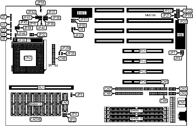
CONNECTIONS | |||
Purpose | Location | Purpose | Location |
PS/2 mouse port | CN1 | Speaker | J2 |
Serial port 1 | CN2 | Turbo switch | J3 |
Serial port 2 | CN3 | Turbo LED | J4 |
Parallel port | CN4 | Reset switch | J5 |
Floppy drive interface | CN5 | Green PC connector | J6 |
IDE interface 1 | CN6 | IDE interface LED | JP35 |
IDE interface 2 | CN7 | 32-bit PCI slots | PC1 - PC4 |
VRM connector | CN8 | Cache slot | SL1 |
Power LED & keylock | J1 | ||
USER CONFIGURABLE SETTINGS | |||
Function | Jumper | Position | |
» | Factory configured - do not alter | JP8 | N/A |
» | Factory configured - do not alter | JP9 | N/A |
» | Factory configured - do not alter | JP10 | N/A |
» | Factory configured - do not alter | JP11 | N/A |
Pipeline disabled | JP42 | Open | |
Pipeline enabled | JP42 | Closed | |
» | Cache type select write back | JP43 | Open |
Cache type select write through | JP43 | Closed | |
» | Factory configured - do not alter | JP48 | N/A |
» | Factory configured - do not alter | JP49 | N/A |
» | CMOS memory normal operation | JP54 | Open |
CMOS memory clear | JP54 | Closed | |
Note: The location of the factory configured jumpers are unidentified. | |||
DRAM CONFIGURATION | ||
Size | Bank 0 | Bank 1 |
8MB | (2) 1M x 36 | NONE |
8MB | (2) 512K x 36 | (2) 512K x 36 |
10MB | (2) 1M x 36 | (2) 256K x 36 |
10MB | (2) 256K x 36 | (2) 1M x 36 |
12MB | (2) 1M x 36 | (2) 512K x 36 |
12MB | (2) 512K x 36 | (2) 1M x 36 |
16MB | (2) 2M x 36 | NONE |
16MB | (2) 1M x 36 | (2) 1M x 36 |
18MB | (2) 2M x 36 | (2) 256K x 36 |
18MB | (2) 256K x 36 | (2) 2M x 36 |
20MB | (2) 2M x 36 | (2) 512K x 36 |
20MB | (2) 512K x 36 | (2) 2M x 36 |
24MB | (2) 2M x 36 | (2) 1M x 36 |
24MB | (2) 1M x 36 | (2) 2M x 36 |
32MB | (2) 4M x 36 | NONE |
32MB | (2) 2M x 36 | (2) 2M x 36 |
34MB | (2) 4M x 36 | (2) 256K x 36 |
34MB | (2) 256K x 36 | (2) 4M x 36 |
36MB | (2) 4M x 36 | (2) 512K x 36 |
36MB | (2) 512K x 36 | (2) 4M x 36 |
40MB | (2) 4M x 36 | (2) 1M x 36 |
40MB | (2) 1M x 36 | (2) 4M x 36 |
48MB | (2) 4M x 36 | (2) 2M x 36 |
48MB | (2) 2M x 36 | (2) 4M x 36 |
64MB | (2) 8M x 36 | NONE |
64MB | (2) 4M x 36 | (2) 4M x 36 |
66MB | (2) 8M x 36 | (2) 256K x 36 |
DRAM CONFIGURATION (CON’T) | ||
Size | Bank 0 | Bank 1 |
66MB | (2) 256K x 36 | (2) 8M x 36 |
68MB | (2) 8M x 36 | (2) 512K x 36 |
68MB | (2) 512K x 36 | (2) 8M x 36 |
72MB | (2) 8M x 36 | (2) 1M x 36 |
72MB | (2) 1M x 36 | (2) 8M x 36 |
80MB | (2) 8M x 36 | (2) 2M x 36 |
80MB | (2) 2M x 36 | (2) 8M x 36 |
96MB | (2) 8M x 36 | (2) 4M x 36 |
96MB | (2) 4M x 36 | (2) 8M x 36 |
128MB | (2) 8M x 36 | (2) 8M x 36 |
CACHE CONFIGURATION | |||
Size | Bank 0 | TAG | SL1 |
256KB (A) | (8) 32K x 8 | (1) 8K/16K/32K x 8 | Not installed |
256KB (B) | NONE | NONE | Installed |
512KB (A) | (8) 64K x 8 | (1) 16K/32K x 8 | Not installed |
512KB (B) | NONE | NONE | Installed |
CACHE JUMPER CONFIGURATION | |||
Size | JP5 | JP36 | JP37 |
256KB | pins 2 & 3 closed | pins 2 & 3 closed | pins 1 & 2 closed |
512KB | pins 1 & 2 closed | pins 1 & 2 closed | pins 2 & 3 closed |
Note: These settings are only valid if standard cache is installed. | |||
CACHE CONFIGURATION | |
Type | JP38 |
Standard cache | pins 1 & 2 closed |
Pipeline burst cache | pins 2 & 3 closed |
CACHE VOLTAGE CONFIGURATION | ||
Voltage | JP3 | JP4 |
Mixed voltage | pins 1 & 2 closed | pins 1 & 2 closed |
3.3v | pins 2 & 3 closed | pins 2 & 3 closed |
CPU TYPE CONFIGURATION | ||
Type | CN8 | JP32 |
P54CX | pins A6 & A7, B6 & B7 closed | Open |
P55C 2.5v | Open | pins 1 & 2, 3 & 4, 5 & 6 closed |
P55C 2.5v on VRM | VRM installed | Open |
P55CT | VRM installed | Open |
CPU SPEED CONFIGURATION | |||||
Speed | JP28 | JP29 | JP31 | JP40 | JP41 |
75MHz | Open | Open | 1 & 2 | 1 & 2 | 1 & 2 |
90MHz | Open | Closed | 2 & 3 | 1 & 2 | 1 & 2 |
100MHz | Closed | Closed | 2 & 3 | 1 & 2 | 1 & 2 |
120MHz | Open | Closed | 2 & 3 | 1 & 2 | 2 & 3 |
133MHz | Closed | Closed | 2 & 3 | 1 & 2 | 2 & 3 |
150MHz | Open | Closed | 2 & 3 | 2 & 3 | 2 & 3 |
Note: Pins designated should be in the closed position. | |||||
CPU VOLTAGE CONFIGURATION | |||
Voltage | JP44 | JP45 | JP46 |
3.3v | Closed | Open | Open |
3.45v - 3.6v | Open | Closed | Open |
DMA CONFIGURATION | |||
» DMA | JP6 | JP7 | |
| » | DMA 1 | pins 2 & 3 closed | pins 2 & 3 closed |
| » | DMA 3 | pins 1 & 2 closed | pins 1 & 2 closed |
PS/2 MOUSE CONFIGURATION | |||||
Setting | JP19 | JP20 | JP21 | JP22 | JP23 |
Disabled | 2 & 3 | 2 & 3 | 2 & 3 | 2 & 3 | 2 & 3 |
Enabled | 1 & 2 | 1 & 2 | 1 & 2 | 1 & 2 | 1 & 2 |
Note: Pins designated should be in the closed position. | |||||
FLASH BIOS CONFIGURATION | ||
Setting | JP50 | JP51 |
Normal mode | pins 2 & 3 closed | pins 2 & 3 closed |
Programming mode | pins 1 & 2 closed | pins 1 & 2 closed |
MISCELLANEOUS TECHNICAL NOTE |
Note: The location of some pin 1’s are unidentified. |
My Books

