MAXSYS 462, 4/100 VL Motherboard Settings and Configuration
CSS LABORATORIES, INC.
MAXSYS 462, 4/100 VL
Processor | 80486SX/80487SX/80486DX/80486DX2/Pentium Overdrive |
Processor Speed | 25/33/50(internal)/50/66(internal)MHz |
Chip Set | OPTI |
Max. Onboard DRAM | 256MB |
Cache | 64/128/256/512KB |
BIOS | Unidentified |
Dimensions | 355mm x 305mm |
I/O Options | 32-bit VESA local bus slot, CPU slot, floppy drive interface, IDE interface, parallel port, auxiliary parallel port, serial ports (2), auxiliary serial ports (2), auxiliary keyboard connectors (2) |
NPU Options | 4167 |
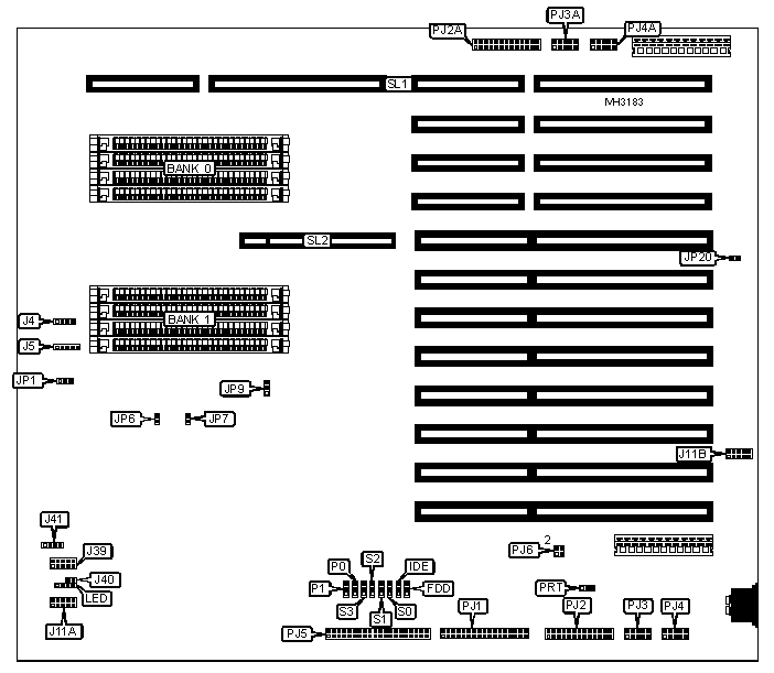
CONNECTIONS | |||
Purpose | Location | Purpose | Location |
Speaker | J4 | Parallel port | PJ2 |
Power LED & keylock | J5 | Serial port 1 | PJ3 |
Front panel connector | J39 | Serial port 2 | PJ4 |
External IDE interface LED | J40 | IDE interface | PJ5 |
Reset switch | J41 pins 1 & 2 | Auxiliary parallel port | PJ2A |
Turbo switch | J41 pins 3 & 4 | Auxiliary serial port 1 | PJ3A |
Auxiliary keyboard connector | J11B | Auxiliary serial port 2 | PJ4A |
Auxiliary keyboard connector | J11A | CPU slot | SL1 |
IDE interface LED | LED | 32-bit VESA local bus slot | SL2 |
Floppy drive interface | PJ1 | ||
USER CONFIGURABLE SETTINGS | |||
Function | Jumper | Position | |
Floppy drive interface enabled | FDD | pins 2 & 3 closed | |
Floppy drive interface disabled | FDD | pins 1 & 2 closed | |
IDE interface enabled | IDE | pins 2 & 3 closed | |
IDE interface disabled | IDE | pins 1 & 2 closed | |
» | CPU type select synchronous | JP1 | pins 1 & 2 closed |
CPU type select asynchronous | JP1 | pins 2 & 3 closed | |
Monitor type select color | JP9 | pins 2 & 3 closed | |
Monitor type select monochrome | JP9 | pins 1 & 2 closed | |
» | Factory configured - do not alter | JP20 | Open |
DRAM CONFIGURATION | ||||
Size | Bank 0 | Bank 1 | Bank 2 | Bank 3 |
4MB | (4) 1M x 9 | NONE | NONE | NONE |
8MB | (4) 1M x 9 | (4) 1M x 9 | NONE | NONE |
12MB | (4) 1M x 9 | (4) 1M x 9 | (4) 1M x 9 | NONE |
16MB | (4) 1M x 9 | (4) 1M x 9 | (4) 1M x 9 | (4) 1M x 9 |
16MB | (4) 4M x 9 | NONE | NONE | NONE |
20MB | (4) 1M x 9 | (4) 4M x 9 | NONE | NONE |
24MB | (4) 1M x 9 | (4) 1M x 9 | (4) 4M x 9 | NONE |
24MB | (4) 1M x 9 | (4) 4M x 9 | (4) 1M x 9 | NONE |
28MB | (4) 1M x 9 | (4) 1M x 9 | (4) 4M x 9 | (4) 1M x 9 |
28MB | (4) 1M x 9 | (4) 4M x 9 | (4) 1M x 9 | (4) 1M x 9 |
32MB | (4) 4M x 9 | (4) 4M x 9 | NONE | NONE |
36MB | (4) 1M x 9 | (4) 4M x 9 | (4) 4M x 9 | NONE |
36MB | (4) 4M x 9 | (4) 4M x 9 | (4) 1M x 9 | NONE |
40MB | (4) 1M x 9 | (4) 1M x 9 | (4) 4M x 9 | (4) 4M x 9 |
40MB | (4) 1M x 9 | (4) 4M x 9 | (4) 4M x 9 | (4) 1M x 9 |
40MB | (4) 4M x 9 | (4) 4M x 9 | (4) 1M x 9 | (4) 1M x 9 |
48MB | (4) 4M x 9 | (4) 4M x 9 | (4) 4M x 9 | NONE |
52MB | (4) 1M x 9 | (4) 4M x 9 | (4) 4M x 9 | (4) 4M x 9 |
Note: Banks 2 & 3 are located on the CPU card. | ||||
DRAM CONFIGURATION (CON’T) | ||||
Size | Bank 0 | Bank 1 | Bank 2 | Bank 3 |
52MB | (4) 4M x 9 | (4) 4M x 9 | (4) 4M x 9 | (4) 1M x 9 |
64MB | (4) 4M x 9 | (4) 4M x 9 | (4) 4M x 9 | (4) 4M x 9 |
64MB | (4) 16M x 9 | NONE | NONE | NONE |
128MB | (4) 16M x 9 | (4) 16M x 9 | NONE | NONE |
192MB | (4) 16M x 9 | (4) 16M x 9 | (4) 16M x 9 | NONE |
256MB | (4) 16M x 9 | (4) 16M x 9 | (4) 16M x 9 | (4) 16M x 9 |
Note: Banks 2 & 3 are located on the CPU card. | ||||
CPU SPEED CONFIGURATION | ||
Speed | JP6 | JP7 |
25MHz | Open | Open |
33MHz | Open | Closed |
50iMHz | Open | Open |
50MHz | Closed | Closed |
66iMHz | Open | Closed |
Note: See also JP1 in User Configurable Settings. | ||
PARALLEL PORT CONFIGURATION | |||||
LPT | IRQ | I/O address | PRT | P0 | P1 |
N/A | N/A | Disabled | N/A | 1 & 2 | 1 & 2 |
LPT1 | IRQ7 | 3BCh | 2 & 3 | 2 & 3 | 1 & 2 |
LPT2 | IRQ5 | 278h | 1 & 2 | 2 & 3 | 2 & 3 |
LPT3 | IRQ7 | 378h | 2 & 3 | 1 & 2 | 2 & 3 |
Note: Pins designated should be in the closed position | |||||
SERIAL PORT 1 CONFIGURATION | |||||
COM | IRQ | I/O address | PJ6 | S0 | S1 |
N/A | N/A | Disabled | N/A | 1 & 2 | 1 & 2 |
COM 1 | IRQ4 | 3F8h | 1 & 2 | 2 & 3 | 2 & 3 |
COM 2 | IRQ3 | 2F8h | 1 & 3 | 1 & 2 | 2 & 3 |
Note: Pins designated should be in the closed position | |||||
SERIAL PORT 2 CONFIGURATION | |||||
COM | IRQ | I/O address | PJ6 | S2 | S3 |
N/A | N/A | Disabled | N/A | 1 & 2 | 1 & 2 |
COM 1 | IRQ4 | 3F8h | 2 & 4 | 1 & 2 | 2 & 3 |
COM 2 | IRQ3 | 2F8h | 3 & 4 | 2 & 3 | 2 & 3 |
Note: Pins designated should be in the closed position | |||||
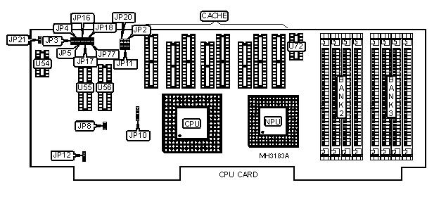
USER CONFIGURABLE SETTINGS | |||
Function | Jumper | Position | |
» | Factory configured - do not alter | JP8 | N/A |
» | Factory configured - do not alter | JP77 | N/A |
CACHE CONFIGURATION | ||
Size | Bank 0 | Bank 1 |
64KB | (4) 8K x 8 | (4) 8K x 8 |
128KB | (4) 32K x 8 | NONE |
256KB | (4) 32K x 8 | (4) 32K x 8 |
512KB | (4) 128K x 8 | NONE |
CACHE TAG CONFIGURATION | ||||
Size | TAG (U54) | TAG (U55) | TAG (U56) | TAG (U72) |
64KB | NONE | (1) 8K x 8 | NONE | (1) 16K/64K x 1 |
128KB | NONE | (1) 8K x 8 | NONE | (1) 16K/64K x 1 |
256KB | NONE | (1) 8K x 8 | (1) 8K x 8 | (1) 16K/64K x 8 |
512KB | NONE | (1) 32K x 8 | NONE | (1) 64K x 1 |
CACHE JUMPER CONFIGURATION | |||||||
Size | JP2 | JP3 | JP4 | JP5 | JP16 | JP17 | JP18 |
64KB | 2 & 3 | Open | Open | Open | Open | Open | Open |
128KB | 1 & 2 | Closed | Open | Open | Closed | Open | Open |
256KB | 2 & 3 | Closed | Closed | Open | Closed | Closed | Open |
512KB | 1 & 2 | Closed | Closed | Closed | Closed | Closed | Closed |
Note: Pins designated should be in the closed position. | |||||||
CPU TYPE CONFIGURATION | ||
Type | JP10 | JP11 |
80486SX | pins 2 & 3 closed | Open |
80487SX | pins 1 & 2, 3 & 4 closed | pins 1 & 2 closed |
80486DX | pins 1 & 2, 3 & 4 closed | pins 2 & 3 closed |
80486DX2 | pins 1 & 2, 3 & 4 closed | pins 2 & 3 closed |
Pentium Overdrive | pins 1 & 2, 3 & 4 closed | pins 1 & 2 closed |
CPU SPEED CONFIGURATION | |
Speed | JP12 |
25MHz | pins 2 & 3 closed |
33MHz | pins 2 & 3 closed |
50iMHz | pins 2 & 3 closed |
50MHz | pins 1 & 2 closed |
66iMHz | pins 2 & 3 closed |
BASE MEMORY CONFIGURATION | ||
Size | JP20 | JP21 |
384KB | pins 2 & 3 closed | Open |
512KB | pins 2 & 3 closed | Closed |
640KB | pins 1 & 2 closed | Any setting |
My Books

