PREFERRED C320SX Motherboard Settings and Configuration
CSS LABORATORIES, INC.
PREFERRED C320SX
Processor | 80386SX |
Processor Speed | 20MHz |
Chip Set | C & T |
Max. Onboard DRAM | 16MB |
SRAM Cache | 16/32KB |
BIOS | AMI |
Dimensions | 330mm x 218mm |
I/O Options | IDE interface, floppy drive interface parallel port, serial port (2) |
NPU Options | 80387SX |
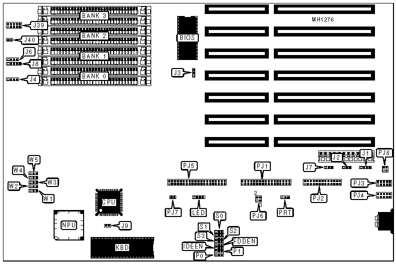
CONNECTIONS | |||
Purpose | Location | Purpose | Location |
External battery | J1 | IDE interface LED | LED |
Reset switch | J4/pins 1 & 2 | Floppy drive interface | PJ1 |
Turbo LED | J4/pins 3 & 4 | Parallel port | PJ2 |
Speaker | J6 | Serial port 1 | PJ3 |
Power LED & keylock | J8 | Serial port 2 | PJ4 |
Front panel switches & LEDs | J39 | IDE interface | PJ5 |
Hard drive access LED | J40 | ||
USER CONFIGURABLE SETTINGS | |||
Function | Jumper | Position | |
| » | Floppy drive interface enabled | FDDEN | pins 2 & 3 closed |
Floppy drive interface disabled | FDDEN | pins 1 & 2 closed | |
| » | IDE interface enabled | IDEEN | pins 2 & 3 closed |
IDE interface disabled | IDEEN | pins 1 & 2 closed | |
| » | CMOS memory normal operation | J2 | pins 2 & 3 closed |
CMOS memory clear | J2 | pins 1 & 2 closed | |
| » | I/O bus wait state select one | J3 | open |
| I/O bus wait states select zero | J3 | pins 2 & 3 closed | |
| » | Monitor type select color | J7 | pins 2 & 3 closed |
Monitor type select monochrome | J7 | pins 1 & 2 closed | |
| » | Factory configured - do not alter | J9 | open |
| » | Factory configured - do not alter | PJ7 | open |
| » | Factory configured - do not alter | PJ8 | open |
DRAM CONFIGURATION | ||||
Size | Bank 0 | Bank 1 | Bank 2 | Bank 3 |
1MB | (2) 256K x 9 | (2) 256K x 9 | NONE | NONE |
2MB | (2) 256K x 9 | (2) 256K x 9 | (2) 256K x 9 | (2) 256K x 9 |
2MB | (2) 1M x 9 | NONE | NONE | NONE |
4MB | (2) 1M x 9 | (2) 1M x 9 | NONE | NONE |
5MB | (2) 1M x 9 | (2) 1M x 9 | (2) 256K x 9 | (2) 256K x 9 |
6MB | (2) 1M x 9 | (2) 1M x 9 | (2) 1M x 9 | NONE |
8MB | (2) 1M x 9 | (2) 1M x 9 | (2) 1M x 9 | (2) 1M x 9 |
8MB | (2) 4M x 9 | NONE | NONE | NONE |
9MB | (2) 4M x 9 | (2) 256K x 9 | (2) 256K x 9 | NONE |
10MB | (2) 4M x 9 | (2) 1M x 9 | NONE | NONE |
11MB | (2) 4M x 9 | (2) 1M x 9 | (2) 256K x 9 | (2) 256K x 9 |
12MB | (2) 4M x 9 | (2) 1M x 9 | (2) 1M x 9 | NONE |
14MB | (2) 4M x 9 | (2) 1M x 9 | (2) 1M x 9 | (2) 1M x 9 |
16MB | (2) 4M x 9 | (2) 4M x 9 | NONE | NONE |
SRAM CONFIGURATION | |||
Size | Cache SRAM | Location | TAG |
16KB | (8) 16K x 1 | Banks 0 & 1 | (1) 8K x 8 |
32KB | (4) 8K x 8 | Bank 0 | (1) 8K x 8 |
Note:Location and configuration of Cache is unverified. | |||
SRAM JUMPER CONFIGURATION | |||||
Size | Jumper W1 | Jumper W2 | Jumper W3 | Jumper W4 | Jumper W5 |
16KB | pins 1 & 2 | pins 1 & 2 | pins 1 & 2 | pins 1 & 2 | pins 1 & 2 |
32KB | pins 2 & 3 | pins 2 & 3 | pins 2 & 3 | pins 2 & 3 | pins 2 & 3 |
Note:Pins designated should be in the closed position. | |||||
SERIAL PORT 1 (PJ3) CONFIGURATION | |||||
COM | IRQ Interrupt | I/O Address | Jumper PJ6 | S0 | S1 |
COM 2 | IRQ3 | 2F8h | pins 1 & 3 | pins 1 & 2 | pins 2 & 3 |
COM 1 | IRQ4 | 3F8h | pins 1 & 2 | pins 2 & 3 | pins 2 & 3 |
Disabled | N/A | N/A | N/A | pins 1 & 2 | pins 1 & 2 |
Note:Pins designated should be in the closed position. | |||||
SERIAL PORT 2 (PJ4) CONFIGURATION | |||||
COM | IRQ Interrupt | I/O Address | Jumper PJ6 | S2 | S3 |
COM 1 | IRQ4 | 3F8h | pins 2 & 4 | pins 1 & 2 | pins 2 & 3 |
COM 2 | IRQ3 | 2F8h | pins 3 & 4 | pins 2 & 3 | pins 2 & 3 |
Disabled | N/A | N/A | N/A | pins 1 & 2 | pins 1 & 2 |
Note:Pins designated should be in the closed position. | |||||
PARALLEL PORT 1 (PJ2) CONFIGURATION | |||||
LPT | IRQ Interrupt | I/O Address | Jumper P0 | Jumper P1 | Jumper PRT |
LPT 1 | IRQ7 | 3F8h | pins 1 & 2 | pins 2 & 3 | pins 2 & 3 |
LPT 2 | IRQ5 | 2F8h | pins 2 & 3 | pins 2 & 3 | pins 1 & 2 |
LPT 3 | IRQ7 | 3BCh | pins 2 & 3 | pins 1 & 2 | pins 2 & 3 |
Disabled | N/A | N/A | pins 1 & 2 | pins 1 & 2 | N/A |
Note:Pins designated should be in the closed position. | |||||
My Books

