SBC-410 Motherboard Settings and Configuration
AAEON TECHNOLOGY, INC.
SBC-410
Device Type | Single board computer |
Processor | 80486SX/CX486DX2/IBM486DX2/ST486DX2/TI486DX2/AM486DE2/ AM486DX2/80486DX2/CX486DX4/IBM486DX4/ST486DX4/ AM486DX4/80486DX4/P24D/P24T/CX5X86/IBM5X86/ST5X86/ AM DX5 |
Processor Speed | 25/33/40/50(internal)/50/66(internal)/75(internal)/100(internal)MHz |
Chip Set | ALI M1489 |
Maximum Onboard Memory | 64MB (EDO supported) |
Cache | 128/256/512KB |
BIOS | AMI |
Dimensions | 185mm x 122mm |
I/O Options | Floppy drive interface, IDE interfaces (2), parallel port, serial ports (2), PC/104 connectors (2) |
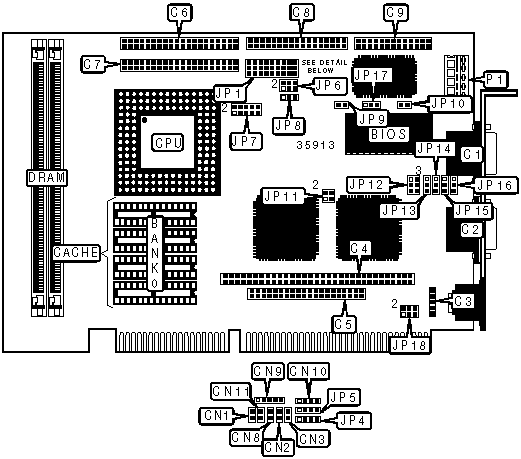
CONNECTIONS | |||
Purpose | Location | Purpose | Location |
Serial port 1 | C1 | Reset switch | CN1 |
Serial port 2 | C2 | Turbo LED | CN2 |
Auxiliary keyboard connector | C3 | IDE interface LED | CN3 |
PC/104 connector | C4 | Turbo switch | CN8 |
PC/104 connector | C5 | Power LED & keylock | CN9 |
IDE interface 1 | C6 | Speaker | CN10 |
IDE interface 2 | C7 | Green PC connector | CN11 |
Floppy drive interface | C8 | 5v power | P1 |
Parallel port | C9 | ||
USER CONFIGURABLE SETTINGS | |||
Function | Label | Position | |
» | Watchdog timer reset | JP4 | Pins 1 & 2 closed |
Watchdog timer IRQ15 | JP4 | Pins 2 & 3 closed | |
» | Factory configured - do not alter | JP5 | Unidentified |
» | CMOS memory normal operation | JP9 | Open |
CMOS memory clear | JP9 | Closed | |
» | Flash BIOS write protect enabled | JP10 | Open |
Flash BIOS write protect disabled | JP10 | Closed | |
» | Flash BIOS voltage select 5v | JP17 | Pins 1 & 2 closed |
Flash BIOS voltage select 12v | JP17 | Pins 2 & 3 closed | |
» | Keyboard connector select used as keyboard | JP18 | Pins 1 & 3, 2 & 4 closed |
Keyboard connector select used as mouse | JP18 | Pins 3 & 5, 4 & 6 closed | |
SIMM CONFIGURATION | ||
Size | Bank 0 | Bank 1 |
1MB | (1) 256K x 36 | None |
2MB | (1) 512K x 36 | None |
2MB | (1) 256K x 36 | (1) 256K x 36 |
3MB | (1) 512K x 36 | (1) 256K x 36 |
4MB | (1) 1M x 36 | None |
4MB | (1) 512K x 36 | (1) 512K x 36 |
5MB | (1) 1M x 36 | (1) 256K x 36 |
6MB | (1) 1M x 36 | (1) 512K x 36 |
8MB | (1) 2M x 36 | None |
8MB | (1) 1M x 36 | (1) 1M x 36 |
9MB | (1) 2M x 36 | (1) 256K x 36 |
10MB | (1) 2M x 36 | (1) 512K x 36 |
12MB | (1) 2M x 36 | (1) 1M x 36 |
SIMM CONFIGURATION (CON’T) | ||
Size | Bank 0 | Bank 1 |
16MB | (1) 4M x 36 | None |
17MB | (1) 4M x 36 | (1) 256K x 36 |
18MB | (1) 4M x 36 | (1) 512K x 36 |
20MB | (1) 4M x 36 | (1) 1M x 36 |
24MB | (1) 4M x 36 | (1) 2M x 36 |
32MB | (1) 8M x 36 | None |
32MB | (1) 4M x 36 | (1) 4M x 36 |
33MB | (1) 8M x 36 | (1) 256K x 36 |
34MB | (1) 8M x 36 | (1) 512K x 36 |
36MB | (1) 8M x 36 | (1) 1M x 36 |
40MB | (1) 8M x 36 | (1) 2M x 36 |
48MB | (1) 8M x 36 | (1) 4M x 36 |
64MB | (1) 8M x 36 | (1) 8M x 36 |
Note: Board accepts EDO memory. | ||
CACHE CONFIGURATION | ||
Size | Bank 0 | TAG |
128KB | (4) 32K x 8 | (1) 32K x 8 |
256KB | (4) 64K x 8 | (1) 32K x 8 |
512KB | (4) 128K x 8 | (1) 32K x 8 |
Note: The location of the TAG is unidentified. | ||
CACHE JUMPER CONFIGURATION | |
Size | JP11 |
128KB | Open |
256KB | Pins 3 & 4 closed |
512KB | Pins 1 & 2, 3 & 4 closed |
CPU SPEED SELECTION | ||
Speed | JP6 | JP8 |
25MHz | Open | Pins 1 & 2 closed |
33MHz | Pins 1 & 2, 3 & 4 closed | Pins 1 & 2 closed |
40MHz | Pins 3 & 4, 5 & 6 closed | Pins 2 & 3 closed |
50iMHz | Open | Pins 1 & 2 closed |
50MHz | Pins 1 & 2, 5 & 6 closed | Pins 2 & 3 closed |
66iMHz | Pins 1 & 2, 3 & 4 closed | Pins 1 & 2 closed |
75iMHz | Open | Pins 1 & 2 closed |
100iMHz | Pins 1 & 2, 3 & 4 closed | Pins 1 & 2 closed |
CPU TYPE SELECTION | |
Type | JP1 |
80486SX | 1 & 4, 2 & 5, 8 & 9, 14 & 17, 19 & 20, 23 & 24, 25 & 26 |
CX 486DX2 | 1 & 4, 2 & 3, 5 & 8, 7 & 10, 11 & 13, 18 & 21, 22 & 23, 25 & 26 |
IBM 486DX2 | 1 & 4, 2 & 3, 5 & 8, 7 & 10, 11 & 13, 18 & 21, 22 & 23, 25 & 26 |
ST 486DX2 | 1 & 4, 2 & 3, 5 & 8, 7 & 10, 11 & 13, 18 & 21, 22 & 23, 25 & 26 |
TI 486DX2 | 1 & 4, 2 & 3, 5 & 8, 7 & 10, 11 & 13, 18 & 21, 22 & 23, 25 & 26 |
AM486DE2 | 1 & 4, 2 & 5, 8 & 9, 10 & 11, 14 & 17, 18 & 21, 19 & 20, 22 & 23, 26 & 27 |
AM486DX2(WB) | 1 & 4, 2 & 5, 8 & 9, 10 & 11, 13 & 16, 14 & 17, 18 & 21, 19 & 20, 22 & 23, 26 & 27 |
AM486DX2(WT) | 1 & 4, 2 & 5, 3 & 6, 8 & 9, 10 & 11, 14 & 17, 18 & 21, 19 & 20, 22 & 23, 26 & 27 |
80486DX2 | 1 & 4, 2 & 5, 8 & 9, 10 & 11, 14 & 17, 18 & 21, 19 & 20, 22 & 23, 26 & 27 |
CX 486DX4 | 1 & 4, 2 & 5, 8 & 9, 10 & 11, 14 & 17, 18 & 21, 19 & 20, 22 & 23, 25 & 26 |
IBM 486DX4 | 1 & 4, 2 & 5, 8 & 9, 10 & 11, 14 & 17, 18 & 21, 19 & 20, 22 & 23, 25 & 26 |
ST 486DX4 | 1 & 4, 2 & 5, 8 & 9, 10 & 11, 14 & 17, 18 & 21, 19 & 20, 22 & 23, 25 & 26 |
AM486DX4 | 1 & 4, 2 & 5, 8 & 9, 10 & 11, 14 & 17, 18 & 21, 19 & 20, 22 & 23, 26 & 27 |
80486DX4 | 1 & 4, 2 & 5, 8 & 9, 10 & 11, 14 & 17, 18 & 21, 19 & 20, 22 & 23, 26 & 27 |
P24D | 1 & 4, 2 & 5, 8 & 9, 10 & 11, 14 & 17, 18 & 21, 19 & 20, 22 & 23, 26 & 27 |
P24T | 1 & 4, 2 & 5, 7 & 10, 8 & 9, 14 & 17, 15 & 18, 19 & 20, 22 & 23, 26 & 27 |
CX 5X86 | 1 & 4, 2 & 5, 8 & 9, 10 & 11, 14 & 17, 18 & 21, 19 & 20, 22 & 23, 25 & 26 |
IBM 5X86 | 1 & 4, 2 & 5, 8 & 9, 10 & 11, 14 & 17, 18 & 21, 19 & 20, 22 & 23, 25 & 26 |
ST 5X86 | 1 & 4, 2 & 5, 8 & 9, 10 & 11, 14 & 17, 18 & 21, 19 & 20, 22 & 23, 25 & 26 |
AM DX5 | 1 & 4, 2 & 5, 8 & 9, 10 & 11, 13 & 16, 14 & 17, 18 & 21, 19 & 20, 22 & 23, 26 & 27 |
Note: Pins designated should be in the closed position. | |
CPU VOLTAGE SELECTION | ||
Voltage | JP7 | |
3.3v | Pins 6 & 8 closed | |
| » | 3.45v | Pins 5 & 7 closed |
3.6v | Pins 8 & 10 closed | |
4.0v | Pins 7 & 9 closed | |
5.0v | Pins 1 & 3, 2 & 4 closed | |
SERIAL PORT 2 SELECTION | ||||||
Setting | JP12 | JP13 | JP14 | JP15 | JP16 | |
| » | RS-232 | 1 & 2 | 1 & 2 | 1 & 2 | 1 & 2 | 1 & 2 |
RS-422 | 3 & 4 | 2 & 3 | 2 & 3 | 2 & 3 | 2 & 3 | |
RS-485 | 5 & 6 | 2 & 3 | 2 & 3 | 2 & 3 | 2 & 3 | |
Note: Pins designated should be in the closed position. | ||||||
My Books

