AT-MIO-16X IO card Settings and Configuration
NATIONAL INSTRUMENTS
AT-MIO-16X
Card Type | Analog to digital timing converter |
Chipset Controller | Unidentified |
I/O Options | Analog input, analog output, digital input, digital output |
Maximum DRAM | N/A |
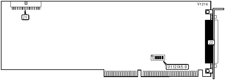
CONNECTIONS | |||
Purpose | Location | Purpose | Location |
34-pin interface connector | J1 | 50-pin I/O connector | J2 |
BASE I/O ADDRESS SELECTION | ||||||
| Address | U112/A5 | U112/A6 | U112/A7 | U112/A8 | U112/A9 | |
| » | 220h | On | Off | Off | Off | On |
| 100h | Off | Off | Off | On | Off | |
| 120h | On | Off | Off | On | Off | |
| 140h | Off | On | Off | On | Off | |
| 160h | On | On | Off | On | Off | |
| 180h | Off | Off | On | On | Off | |
| 360h | On | On | Off | On | On | |
| 380h | Off | Off | On | On | On | |
| 3A0h | On | Off | On | On | On | |
| 3C0h | Off | On | On | On | On | |
| 3E0h | On | On | On | On | On | |
Note: A total of 255 base address settings are available. The switches are a binary representation of the decimal memory addresses. Switch A9 is the Most Significant Bit and switch A5 is the Least Significant Bit. The switches have the following decimal values: switch A9=512, A8=256, A7=128, A6=64, A5=32. Turn on the switches and add the values of the switches that are on to obtain the correct memory address. (On=1, Off=0) | ||||||
My Books

