PCI-001V2 Network Card Settings and Configuration
DTK COMPUTER, INC.
PCI-001V2
NIC Type | Arcnet |
Transfer Rate | 2.5Mbps |
Data Bus | 8-bit ISA |
Topology | Linear Bus/Star |
Wiring Type | RG-62A/U 93ohm coaxial |
Boot ROM | Available |
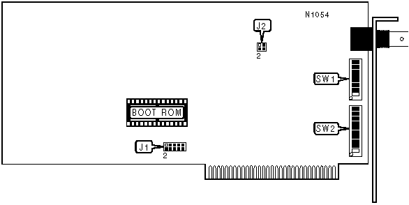
NODE ADDRESS SELECTION | ||||||||
Address | SW1/1 | SW1/2 | SW1/3 | SW1/4 | SW1/5 | SW1/6 | SW1/7 | SW1/8 |
1 | Off | On | On | On | On | On | On | On |
2 | On | Off | On | On | On | On | On | On |
3 | Off | Off | On | On | On | On | On | On |
4 | On | On | Off | On | On | On | On | On |
5 | Off | On | Off | On | On | On | On | On |
251 | Off | Off | On | Off | Off | Off | Off | Off |
252 | On | On | Off | Off | Off | Off | Off | Off |
253 | Off | On | Off | Off | Off | Off | Off | Off |
254 | On | Off | Off | Off | Off | Off | Off | Off |
255 | Off | Off | Off | Off | Off | Off | Off | Off |
Note: A total of 255 node address settings are available. The switches are a binary representation of the decimal node addresses. Switch SW1/1 is the Least Significant Bit and switch SW1/8 is the Most Significant Bit. The switches have the following decimal values: switch SW1/1=1, SW1/2=2, SW1/3=4, SW1/4=8, SW1/5=16, SW1/6=32, SW1/7=64, SW1/8=128. Turn off the switches and add the values of the off switches to obtain the correct node address. (on=0, off=1) | ||||||||
BASE I/O ADDRESS SELECTION | ||||||
Address | SW2/1 | SW2/2 | SW2/3 | SW2/4 | SW2/5 | SW2/6 |
010h | Off | On | On | On | On | On |
020h | On | Off | On | On | On | On |
030h | Off | Off | On | On | On | On |
040h | On | On | Off | On | On | On |
050h | Off | On | Off | On | On | On |
3B0h | Off | Off | On | Off | Off | Off |
3C0h | On | On | Off | Off | Off | Off |
3D0h | Off | On | Off | Off | Off | Off |
3E0h | On | Off | Off | Off | Off | Off |
3F0h | Off | Off | Off | Off | Off | Off |
Note: A total of 63 base I/O address settings are available. The switches are a binary representation of the hexadecimal base I/O addresses. Switch SW2/1 is the Least Significant Bit and switch SW2/8 is the Most Significant Bit. The switches have the following hexadecimal values: switch SW2/1=10h, SW2/2=20h, SW2/3=40h, SW2/4=80h, SW2/5=100h, SW2/6=200h. Turn off the switches and add the values of the off switches to obtain the correct base I/O address. (on=0, off=1) | ||||||
SHARED RAM ADDRESS SELECTION | ||||
Address | SW2/7 | SW2/8 | SW2/9 | SW2/10 |
10000h | Off | On | On | On |
20000h | On | Off | On | On |
30000h | Off | Off | On | On |
40000h | On | On | Off | On |
50000h | Off | On | Off | On |
B0000h | Off | Off | On | Off |
C0000h | On | On | Off | Off |
D0000h | Off | On | Off | Off |
E0000h | On | Off | Off | Off |
F0000h | Off | Off | Off | Off |
Note: A total of 15 shared ram address settings are available. The switches are a binary representation of the hexadecimal shared ram addresses. Switch SW2/7 is the Least Significant Bit and switch SW2/10 is the Most Significant Bit. The switches have the following hexadecimal values: switch SW2/7=10000h, SW2/8=20000h, SW2/9=40000h, SW2/10=80000h. Turn off the switches and add the values of the off switches to obtain the correct shared ram address. (on=0, off=1) | ||||
INTERRUPT SELECTION | |
IRQ | J1 |
2 | pins 1 & 2 closed |
3 | pins 3 & 4 closed |
4 | pins 5 & 6 closed |
5 | pins 7 & 8 closed |
7 | pins 9 & 10 closed |
TIME-OUT CONFIGURATION | |||
Response Time | Idle Time | Reconfiguration Time | J2 |
7.47 m s | 86 m s | 840 m s | Open |
285 m s | 316 m s | 1680 m s | pins 1 & 2 closed |
563 m s | 624 m s | 1680 m s | pins 3 & 4 closed |
1130 m s | 1237 m s | 1680 m s | pins 1 & 2, 3 & 4 closed |
My Books

