PV5000HX Motherboard Settings and Configuration
TEXAS MICROSYSTEMS, INC.
PV5000HX
Processor | Pentium |
Processor Speed | 75/90/100/120/133/150/166/180/200MHz |
Chip Set | Unidentified |
Video Chip Set | Unidentified |
Maximum Onboard Memory | 256MB (EDO supported) |
Maximum Video Memory | Unidentified |
Cache | 256/512KB |
BIOS | Unidentified |
Dimensions | 305mm x 244mm |
I/O Options (CPU) | Floppy drive interface, IDE interface, SCSI interface, parallel port, PS/2 mouse interface, serial ports (2), cache slot |
I/O Options (Backplane) | 32-bit PCI slots (6), CPU slot |
NPU Options | None |
CONNECTIONS | |||
Purpose | Location | Purpose | Location |
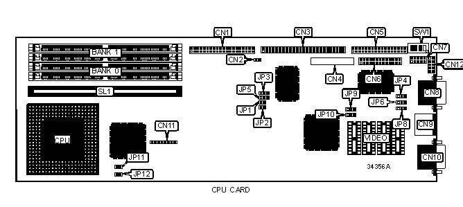
IDE interface | CN1 | VGA port | CN8 |
IDE/SCSI interface LED | CN2 | PS/2 mouse port | CN9 |
SCSI interface | CN3 | Serial port 1 | CN10 |
Flat panel connector | CN4 | AT keyboard connector | CN11 |
Floppy drive interface | CN5 | VGA interface | CN12 |
Parallel port | CN6 | Cache slot | SL1 |
Serial port 2 | CN7 | ||
USER CONFIGURABLE SETTINGS | |||
Function | Label | Position | |
» | Shift clock panel select normal | JP3 | Pins 1 & 2 closed |
Shift clock panel select inverted | JP3 | Pins 2 & 3 closed | |
» | PS/2 IRQ 12 enabled | JP5 | Pins 2 & 3 closed |
Next Step OS used | JP5 | Pins 1 & 2 closed | |
» | LCD bias select negative | JP9 | Pins 1 & 2 closed |
LCD bias select positive | JP9 | Pins 2 & 3 closed | |
» | Panel interface voltage select 5v | JP10 | Pins 1 & 2 closed |
Panel interface voltage select 3.3v | JP10 | Pins 2 & 3 closed | |
» | Monitor type select color | SW1/1 | On |
Monitor type select monochrome | SW1/1 | Off | |
» | Flash BIOS enabled | SW1/2 | Off |
Flash BIOS disabled | SW1/2 | On | |
» | CMOS memory normal operation | SW1/3 | Off |
CMOS memory clear | SW1/3 | On | |
» | I/O address select 270H | SW1/4 | Off |
I/O address select 370H | SW1/4 | On | |
DRAM CONFIGURATION (EDO MEMORY) | ||
Size | Bank 0 | Bank 1 |
8MB | (2) 1M x 32 | None |
16MB | (2) 2M x 32 | None |
16MB | (2) 1M x 32 | (2) 1M x 32 |
24MB | (2) 2M x 32 | (2) 1M x 32 |
32MB | (2) 4M x 32 | None |
32MB | (2) 2M x 32 | (2) 2M x 32 |
40MB | (2) 4M x 32 | (2) 1M x 32 |
48MB | (2) 4M x 32 | (2) 2M x 32 |
64MB | (2) 8M x 32 | None |
64MB | (2) 4M x 32 | (2) 4M x 32 |
72MB | (2) 8M x 32 | (2) 1M x 32 |
80MB | (2) 8M x 32 | (2) 2M x 32 |
96MB | (2) 8M x 32 | (2) 4M x 32 |
128MB | (2) 8M x 32 | (2) 8M x 32 |
DRAM CONFIGURATION (FPM MEMORY) | ||
Size | Bank 0 | Bank 1 |
8MB | (2) 1M x 36 | None |
16MB | (2) 2M x 36 | None |
16MB | (2) 1M x 36 | (2) 1M x 36 |
24MB | (2) 2M x 36 | (2) 1M x 36 |
32MB | (2) 4M x 36 | None |
32MB | (2) 2M x 36 | (2) 2M x 36 |
DRAM CONFIGURATION (FPM MEMORY CON’T) | ||
Size | Bank 0 | Bank 1 |
40MB | (2) 4M x 36 | (2) 1M x 36 |
48MB | (2) 4M x 36 | (2) 2M x 36 |
64MB | (2) 8M x 36 | None |
64MB | (2) 4M x 36 | (2) 4M x 36 |
72MB | (2) 8M x 36 | (2) 1M x 36 |
80MB | (2) 8M x 36 | (2) 2M x 36 |
96MB | (2) 8M x 36 | (2) 4M x 36 |
128MB | (2) 8M x 36 | (2) 8M x 36 |
128MB | (2) 16M x 36 | None |
136MB | (2) 16M x 36 | (2) 1M x 36 |
144MB | (2) 16M x 36 | (2) 2M x 36 |
160MB | (2) 16M x 36 | (2) 4M x 36 |
192MB | (2) 16M x 36 | (2) 8M x 36 |
256MB | (2) 16M x 36 | (2) 16M x 36 |
CACHE CONFIGURATION | |
Size | SL1 |
256KB | 256KB module installed |
512KB | 512KB module installed |
VIDEO MEMORY CONFIGURATION |
Note: The size of the video memory is unidentified. |
CPU SPEED SELECTION | ||||||
CPU speed | Clock speed | Multiplier | JP1 | JP2 | JP11 | JP12 |
75MHz | 50MHz | 1.5x | Closed | Closed | N/A | N/A |
90MHz | 60MHz | 1.5x | Closed | Open | N/A | N/A |
100MHz | 66MHz | 1.5x | Open | Closed | Open | Open |
120MHz | 60MHz | 2x | Closed | Open | N/A | N/A |
133MHz | 66MHz | 2x | Open | Closed | Open | Closed |
150MHz | 60MHz | 2.5x | Closed | Open | N/A | N/A |
166MHz | 66MHz | 2.5x | Open | Closed | Closed | Closed |
180MHz | 60MHz | 3x | Closed | Open | N/A | N/A |
200MHz | 66MHz | 3x | Open | Closed | Closed | Open |
Note: Pins designated should be in the closed position. | ||||||
SERIAL PORT 2 SELECTION | ||||
Setting | JP4 | JP6 | JP8 | |
| » | RS232 | Pins 2 & 3 closed | Pins 2 & 3 closed | Pins 2 & 3 closed |
RS422 | Pins 1 & 2 closed | Pins 1 & 2 closed | Pins 1 & 2 closed | |
RS485 | Pins 1 & 2 closed | Pins 1 & 2 closed | Pins 1 & 2 closed | |
CONNECTIONS | |||
Purpose | Location | Purpose | Location |
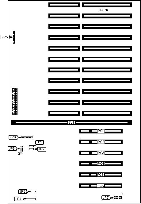
Front keyboard connector | JP4 | Front panel connector | JP8 |
Rear keyboard connector | JP5 | CPU slot | SL1 |
CPU interface | JP6 | ||
USER CONFIGURABLE SETTINGS | |||
Function | Label | Position | |
» | Factory configured - do not alter | JP1 | Unidentified |
» | Factory configured - do not alter | JP2 | Unidentified |
» | Factory configured - do not alter | JP3 | Unidentified |
» | Factory configured - do not alter (PCI J tag) | JP7 | Unidentified |
My Books

