RHINO 6VX Motherboard Settings and Configuration
OCEAN INFORMATION SYSTEMS, INC.
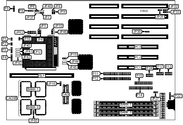
RHINO 6VX
Processor | CX M1/AM K5/Pentium |
Processor Speed | 75/90/100/120/133/150/166/180/200MHz |
Chip Set | Intel |
Video Chip Set | None |
Maximum Onboard Memory | 128MB (EDO supported) |
Maximum Video Memory | None |
Cache | 256/512KB |
BIOS | Award |
Dimensions | 279mm x 216mm |
I/O Options | 32-bit PCI slots (3), floppy drive interface, green PC connector, IDE interfaces (2), parallel port, PS/2 mouse interface, serial ports (2), cache slot, IR connector, VRM connector, USB connector |
NPU Options | None |
CONNECTIONS | |||
Purpose | Location | Purpose | Location |
Reset switch | P1 | Serial port 2 | P13 |
Turbo LED | P2 | Floppy drive interface | P14 |
Speaker | P3 | Parallel port | P15 |
Power LED & keylock | P4 | Serial port 1 | P17 |
IDE interface LED | P5 | PS/2 mouse interface | P22 |
External battery | P9 | USB connector | P24 |
Green PC connector | P10 | 32-bit PCI slots | PC1 - PC3 |
IDE interface 1 | P11 | Cache slot | SL1 |
IDE interface 2 | P12 | ||
USER CONFIGURABLE SETTINGS | |||
Function | Label | Position | |
» | Battery type select internal | JP6 | Pins 1 & 2 closed |
Battery type select external | JP6 | Pins 2 & 3 closed | |
» | CMOS memory normal operation | JP7 | Pins 1 & 2 closed |
CMOS memory clear | JP7 | Pins 2 & 3 closed | |
» | Factory configured - do not alter | JP15 | Pins 1 & 2 closed |
» | Power good signal detect from power supply | JP27 | Pins 1 & 2 closed |
Power good signal detect from board | JP27 | Pins 2 & 3 closed | |
» | Factory configured - do not alter | JP30 | Pins 1 & 2 closed |
» | Factory configured - do not alter | JP37 | Unidentified |
» | Factory configured - do not alter | JP40 | Unidentified |
» | Factory configured - do not alter | JP41 | Unidentified |
» | Factory configured - do not alter | JP42 | Unidentified |
» | Factory configured - do not alter | JP43 | Unidentified |
» | Factory configured - do not alter | JP44 | Unidentified |
» | Factory configured - do not alter | JP45 | Unidentified |
» | Factory configured - do not alter | JP46 | Unidentified |
» | Factory configured - do not alter | JP48 | Unidentified |
DRAM CONFIGURATION | ||
Size | Bank 0 | Bank 1 |
4MB | (2) 512K x 36 | None |
8MB | (2) 1M x 36 | None |
8MB | (2) 512K x 36 | (2) 512K x 36 |
12MB | (2) 1M x 36 | (2) 512K x 36 |
16MB | (2) 2M x 36 | None |
16MB | (2) 1M x 36 | (2) 1M x 36 |
20MB | (2) 2M x 36 | (2) 512K x 36 |
24MB | (2) 1M x 36 | (2) 2M x 36 |
32MB | (2) 4M x 36 | None |
32MB | (2) 2M x 36 | (2) 2M x 36 |
DRAM CONFIGURATION (CON’T) | ||
Size | Bank 0 | Bank 1 |
36MB | (2) 512K x 36 | (2) 4M x 36 |
40MB | (2) 4M x 36 | (2) 1M x 36 |
48MB | (2) 2M x 36 | (2) 4M x 36 |
64MB | (2) 8M x 36 | None |
64MB | (2) 4M x 36 | (2) 4M x 36 |
68MB | (2) 512K x 36 | (2) 8M x 36 |
72MB | (2) 8M x 36 | (2) 1M x 36 |
80MB | (2) 2M x 36 | (2) 8M x 36 |
96MB | (2) 8M x 36 | (2) 4M x 36 |
128MB | (2) 8M x 36 | (2) 8M x 36 |
Note: Board accepts EDO memory. Board also accepts x 32 SIMMs. Banks are interchangeable. | ||
CACHE CONFIGURATION | ||||
Size | Bank 0 | Bank 1 | SL1 | TAG |
256KB | (2) 32K x 32 | None | Not installed | (1) 8K/32K x 8 |
512KB (A) | (2) 32K x 32 | (2) 32K x 32 | Not installed | (1) 32K x 8 |
512KB (B) | (2) 32K x 32 | None | 256KB module installed | (1) 32K x 8 |
CACHE JUMPER CONFIGURATION | ||
Size | JP16 | JP50 |
256KB | Open | Pins 2 & 3 closed |
512KB (A) | Pins 2 & 3 closed | Pins 1 & 2 closed |
512KB (B) | Pins 2 & 3 closed | Pins 1 & 2 closed |
CPU SPEED SELECTION (CYRIX) | |||||||
CPU speed | Clock speed | Multiplier | JP4 | JP5 | JP8 | JP9 | JP10 |
120MHz | 50MHz | 2x | 2 & 3 | 1 & 2 | 2 & 3 | 2 & 3 | 1 & 2 |
133MHz | 55MHz | 2x | 2 & 3 | 1 & 2 | 1 & 2 | 1 & 2 | 1 & 2 |
150MHz | 60MHz | 2x | 2 & 3 | 1 & 2 | 1 & 2 | 2 & 3 | 2 & 3 |
166MHz | 66MHz | 2x | 2 & 3 | 1 & 2 | 2 & 3 | 1 & 2 | 2 & 3 |
Note: Pins designated should be in the closed position. | |||||||
CPU SPEED SELECTION (AMD) | |||||||
CPU speed | Clock speed | Multiplier | JP4 | JP5 | JP8 | JP9 | JP10 |
75MHz | 50MHz | 1.5x | 1 & 2 | 1 & 2 | 2 & 3 | 2 & 3 | 1 & 2 |
90MHz | 60MHz | 1.5x | 1 & 2 | 1 & 2 | 1 & 2 | 2 & 3 | 2 & 3 |
100MHz | 66MHz | 1.5x | 1 & 2 | 1 & 2 | 2 & 3 | 1 & 2 | 2 & 3 |
120MHz | 60MHz | 1.5x | 1 & 2 | 1 & 2 | 1 & 2 | 2 & 3 | 2 & 3 |
133MHz | 66MHz | 1.5x | 1 & 2 | 1 & 2 | 2 & 3 | 1 & 2 | 2 & 3 |
150MHz | 60MHz | 2x | 2 & 3 | 1 & 2 | 1 & 2 | 2 & 3 | 2 & 3 |
Note: Pins designated should be in the closed position. | |||||||
CPU SPEED SELECTION (INTEL) | |||||||
CPU speed | Clock speed | Multiplier | JP4 | JP5 | JP8 | JP9 | JP10 |
75MHz | 50MHz | 1.5x | 1 & 2 | 1 & 2 | 2 & 3 | 2 & 3 | 1 & 2 |
90MHz | 60MHz | 1.5x | 1 & 2 | 1 & 2 | 1 & 2 | 2 & 3 | 2 & 3 |
100MHz | 66MHz | 1.5x | 1 & 2 | 1 & 2 | 2 & 3 | 1 & 2 | 2 & 3 |
120MHz | 60MHz | 2x | 2 & 3 | 1 & 2 | 1 & 2 | 2 & 3 | 2 & 3 |
133MHz | 66MHz | 2x | 2 & 3 | 1 & 2 | 2 & 3 | 1 & 2 | 2 & 3 |
150MHz | 60MHz | 2.5x | 2 & 3 | 2 & 3 | 1 & 2 | 2 & 3 | 2 & 3 |
166MHz | 66MHz | 2.5x | 2 & 3 | 2 & 3 | 2 & 3 | 1 & 2 | 2 & 3 |
180MHz | 60MHz | 3x | 1 & 2 | 2 & 3 | 1 & 2 | 2 & 3 | 2 & 3 |
200MHz | 66MHz | 3x | 1 & 2 | 2 & 3 | 2 & 3 | 1 & 2 | 2 & 3 |
Note: Pins designated should be in the closed position. | |||||||
CPU VOLTAGE SELECTION | ||
Voltage | JP52 | |
| » | 3.3v | Pins 3 & 4 closed |
3.5v | Pins 1 & 2 closed | |
PS/2 MOUSE SELECTION | ||||
Setting | JP31 | JP32 | JP33 | |
| » | Enabled | Pins 1 & 2 closed | Pins 2 & 3 closed | Pins 2 & 3 closed |
Disabled | Pins 2 & 3 closed | Pins 1 & 2 closed | Pins 1 & 2 closed | |
My Books

