MPE-PNTM Motherboard Settings and Configuration
MYLEX CORPORATION
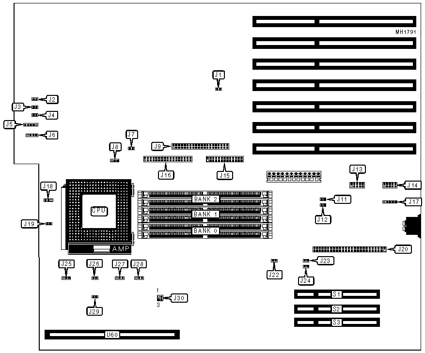
MPE-PNTM
Processor | Pentium |
Processor Speed | 60/66MHz |
Chip Set | Mercury |
Max. onboard DRAM | 192MB |
Cache | 256/512KB |
BIOS | AMI |
Dimensions | 356mm x 304mm |
I/O Options | 32-bit PCI local bus slots (3), floppy drive interface, IDE interface, parallel port, serial ports (2) |
NPU Options | None |
CONNECTIONS | |||
Purpose | Location | Purpose | Location |
Reset switch | J4 | Internal keyboard connector | J17 |
Power LED & keylock | J5 | Chassis fan power | J18 |
Speaker | J6 | SCSI connector | J20 |
IDE interface | J9 | IDE interface LED | J22 |
Serial port 1 | J13 | 32-bit PCI local bus slot | S1 |
Serial port 2 | J14 | 32-bit PCI local bus slot | S2 |
Parallel port | J15 | 32-bit PCI local bus slot | S3 |
Floppy drive interface | J16 | Cache SIMM module | U60 |
USER CONFIGURABLE SETTINGS | |||
Function | Jumper | Position | |
» | IDE DMA disabled | J1 | Open |
| IDE DMA on channel 6 | J1 | Closed |
» | Factory configured - do not alter | J2 | Open |
» | Monitor type select color | J3 | Closed |
| Monitor type select monochrome | J3 | Open |
» | Factory configured - do not alter | J7 | Open |
» | Factory configured - do not alter | J8 | Pins 2 & 3 closed |
» | Factory configured - do not alter | J11 | Open |
» | Factory configured - do not alter | J12 | Open |
» | Write-back cache enabled | J19 | Open |
| Write-thru cache enabled | J19 | Closed |
» | Factory configured - do not alter | J26 | Open |
» | Standard asynchronous SRAM | J28 | Pins 1 & 2 closed |
| Burst synchronous SRAM | J28 | Pins 2 & 3 closed |
» | Factory configured - do not alter | J29 | Open |
» | Cache parity support disabled | J30 | Pins 1 & 2 and 3 & 4 |
| Cache parity support enabled | J30 | Pins 1 & 3 and 2 & 4 |
Note: Pins designated should be in the closed position. | |||
DRAM CONFIGURATION | |||
Size | Bank 0 | Bank 1 | Bank 2 |
2MB | (2) 256K x 36 | NONE | NONE |
4MB | (2) 256K x 36 | (2) 256K x 36 | NONE |
6MB | (2) 256K x 36 | (2) 256K x 36 | (2) 256K x 36 |
8MB | (2) 1M x 36 | NONE | NONE |
10MB | (2) 1M x 36 | (2) 256K x 36 | NONE |
12MB | (2) 1M x 36 | (2) 256K x 36 | (2) 256K x 36 |
16MB | (2) 1M x 36 | (2) 1M x 36 | NONE |
16MB | (2) 2M x 36 | NONE | NONE |
18MB | (2) 1M x 36 | (2) 1M x 36 | (2) 256K x 36 |
18MB | (2) 2M x 36 | (2) 256K x 36 | NONE |
20MB | (2) 2M x 36 | (2) 256K x 36 | (2) 256K x 36 |
24MB | (2) 1M x 36 | (2) 1M x 36 | (2) 1M x 36 |
24MB | (2) 2M x 36 | (2) 1M x 36 | NONE |
DRAM CONFIGURATION | |||
Size | Bank 0 | Bank 1 | Bank 2 |
32MB | (2) 4M x 36 | NONE | NONE |
32MB | (2) 2M x 36 | (2) 1M x 36 | (2) 1M x 36 |
32MB | (2) 2M x 36 | (2) 2M x 36 | NONE |
34MB | (2) 4M x 36 | (2) 256K x 36 | NONE |
40MB | (2) 2M x 36 | (2) 2M x 36 | (2) 1M x 36 |
40MB | (2) 4M x 36 | (2) 1M x 36 | NONE |
48MB | (2) 4M x 36 | (2) 2M x 36 | NONE |
48MB | (2) 2M x 36 | (2) 2M x 36 | (2) 2M x 36 |
64MB | (2) 4M x 36 | (2) 4M x 36 | NONE |
64MB | (2) 2M x 36 | (2) 2M x 36 | (2) 2M x 36 |
64MB | (2) 8M x 36 | NONE | NONE |
66MB | (2) 8M x 36 | (2) 256K x 36 | NONE |
68MB | (2) 8M x 36 | (2) 256K x 36 | (2) 256K x 36 |
72MB | (2) 8M x 36 | (2) 1M x 36 | NONE |
80MB | (2) 8M x 36 | (2) 1M x 36 | (2) 1M x 36 |
80MB | (2) 8M x 36 | (2) 2M x 36 | NONE |
96MB | (2) 8M x 36 | (2) 2M x 36 | (2) 2M x 36 |
96MB | (2) 8M x 36 | (2) 4M x 36 | NONE |
98MB | (2) 8M x 36 | (2) 4M x 36 | (2) 256K x 36 |
104MB | (2) 8M x 36 | (2) 4M x 36 | (2) 1M x 36 |
114MB | (2) 8M x 36 | (2) 4M x 36 | (2) 2M x 36 |
128MB | (2) 8M x 36 | (2) 4M x 36 | (2) 4M x 36 |
128MB | (2) 8M x 36 | (2) 8M x 36 | NONE |
196MB | (2) 8M x 36 | (2) 8M x 36 | (2) 8M x 36 |
CACHE JUMPER CONFIGURATION | |||
Size | J25 | J27 | |
» | 0KB | Pins 1 & 2 closed | Pins 1 & 2 closed |
| 256KB | Pins 1 & 2 closed | Pins 2 & 3 closed |
| 512KB | Pins 2 & 3 closed | Pins 2 & 3 closed |
SCSI INTERFACE CONFIGURATION | ||||
Bus Power | Termination | J23 | J24 | |
» | Internal | Internal | Closed | Open |
| External | External | Closed | Open |
Note:When SCSI cable is connected, J23 and J24 should be closed. | ||||
My Books

