IPC VALUEMAGIC (MB486PCI#10) Motherboard Settings and Configuration
IPC CORPORATION, LTD.
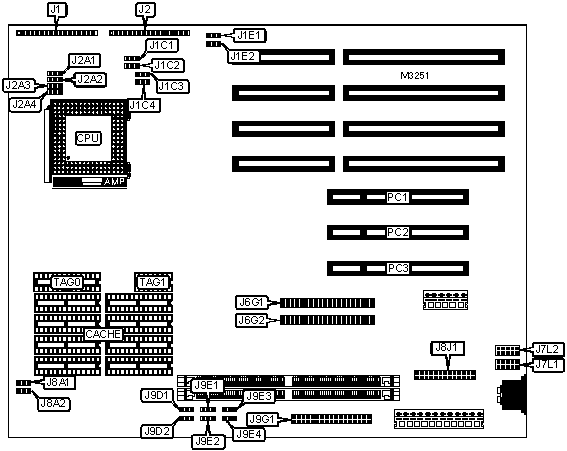
IPC VALUEMAGIC (MB486PCI#10)
Processor | 80486SX/80486SX2/80486DX2/80486DX4 |
Processor Speed | 33/50(internal)/66(internal)/100(internal)MHz |
Chip Set | Intel |
Max. Onboard DRAM | 64MB |
Cache | 128/256KB |
BIOS | AMI |
Dimensions | 330mm x 218mm |
I/O Options | 32-bit PCI slots (3), floppy drive interface, IDE interfaces (2), parallel port, serial ports (2) |
NPU Options | None |
CONNECTIONS | |||
Purpose | Location | Purpose | Location |
Reset switch | J1 pins 1 & 2 | IDE interface | J6G1 |
Power LED & keylock | J1 pins 4 - 8 | IDE interface | J6G2 |
IDE interface LED | J1 pins 10 - 13 | Serial port 1 | J7L1 |
Turbo LED | J1 pins 16 & 17 | Serial port 2 | J7L2 |
Chassis fan power | J2 pins 6 - 8 | Parallel port | J8J1 |
Speaker | J2 pins 10 - 13 | Floppy drive interface | J9G1 |
Turbo switch | J2 pins 16 & 17 | 32-bit PCI slots | PC1 - PC3 |
USER CONFIGURABLE SETTINGS | |||
Function | Jumper | Position | |
» | Factory configured - do not alter | J1C1 | N/A |
» | Password enabled | J9D1 | Pins 1 & 2 closed |
Password disabled | J9D1 | Pins 2 & 3 closed | |
» | Monitor type select color | J9D2 | Pins 1 & 2 closed |
Monitor type select monochrome | J9D2 | Pins 2 & 3 closed | |
» | CMOS memory normal operation | J9E1 | Pins 1 & 2 closed |
CMOS memory clear | J9E1 | Pins 2 & 3 closed | |
» | Setup access enabled | J9E2 | Pins 1 & 2 closed |
Setup access disabled | J9E2 | Pins 2 & 3 closed | |
» | Flash BIOS write protect enabled | J9E3 | Pins 1 & 2 closed |
Flash BIOS write protect disabled | J9E3 | Pins 2 & 3 closed | |
» | Normal boot enabled | J9E4 | Pins 1 & 2 closed |
Recovery boot enabled | J9E4 | Pins 2 & 3 closed | |
DRAM CONFIGURATION | ||
Size | Bank 0 | Bank 1 |
1MB | (1) 256K x 36 | None |
1MB | None | (1) 256K x 36 |
2MB | (1) 256K x 36 | (1) 256K x 36 |
2MB | None | (1) 512K x 36 |
2MB | (1) 512K x 36 | None |
3MB | (1) 512K x 36 | (1) 256K x 36 |
3MB | (1) 256K x 36 | (1) 512K x 36 |
4MB | (1) 512K x 36 | (1) 512K x 36 |
4MB | (1) 1M x 36 | None |
4MB | None | (1) 1M x 36 |
5MB | (1) 256K x 36 | (1) 1M x 36 |
5MB | (1) 1M x 36 | (1) 256K x 36 |
6MB | (1) 1M x 36 | (1) 512K x 36 |
6MB | (1) 512K x 36 | (1) 1M x 36 |
8MB | (1) 1M x 36 | (1) 1M x 36 |
8MB | (1) 2M x 36 | None |
8MB | None | (1) 2M x 36 |
9MB | (1) 2M x 36 | (1) 256K x 36 |
9MB | (1) 256K x 36 | (1) 2M x 36 |
10MB | (1) 2M x 36 | (1) 512K x 36 |
10MB | (1) 512K x 36 | (1) 2M x 36 |
12MB | (1) 2M x 36 | (1) 1M x 36 |
12MB | (1) 1M x 36 | (1) 2M x 36 |
16MB | (1) 2M x 36 | (1) 2M x 36 |
16MB | (1) 4M x 36 | None |
16MB | None | (1) 4M x 36 |
17MB | (1) 4M x 36 | (1) 256K x 36 |
DRAM CONFIGURATION (CON’T) | ||
Size | Bank 0 | Bank 1 |
17MB | (1) 256K x 36 | (1) 4M x 36 |
18MB | (1) 4M x 36 | (1) 512K x 36 |
18MB | (1) 512K x 36 | (1) 4M x 36 |
20MB | (1) 1M x 36 | (1) 4M x 36 |
20MB | (1) 4M x 36 | (1) 1M x 36 |
24MB | (1) 4M x 36 | (1) 2M x 36 |
24MB | (1) 2M x 36 | (1) 4M x 36 |
32MB | (1) 4M x 36 | (1) 4M x 36 |
32MB | (1) 8M x 36 | None |
33MB | (1) 256K x 36 | (1) 8M x 36 |
33MB | (1) 8M x 36 | (1) 256K x 36 |
34MB | (1) 512K x 36 | (1) 8M x 36 |
34MB | (1) 8M x 36 | (1) 512K x 36 |
36MB | (1) 8M x 36 | (1) 1M x 36 |
36MB | (1) 1M x 36 | (1) 8M x 36 |
40MB | (1) 8M x 36 | (1) 2M x 36 |
40MB | (1) 2M x 36 | (1) 8M x 36 |
48MB | (1) 8M x 36 | (1) 4M x 36 |
48MB | (1) 4M x 36 | (1) 8M x 36 |
64MB | (1) 8M x 36 | (1) 8M x 36 |
Note: The orientation of Banks 0 & 1 are unidentified. | ||
CACHE CONFIGURATION | ||||
Size | Bank 0 | Bank 1 | TAG0 | TAG1 |
128KB | (4) 32K x 8 | None | (1) 32K x 8 | (1) 16K x 1 |
256KB | (4) 32K x 8 | (4) 32K x 8 | (1) 32K x 8 | (1) 16K x 1 |
Note: The orientation of Banks 0 & 1 are unidentified. | ||||
CACHE JUMPER CONFIGURATION | ||
Size | J8A1 | J8A2 |
128KB | Pins 2 & 3 closed | Pins 2 & 3 closed |
256KB | Pins 1 & 2 closed | Pins 1 & 2 closed |
CPU TYPE CONFIGURATION | |||||
Type | J1E1 | J1E2 | J1C2 | J1C3 | J1C4 |
80486SX-33 | 1 & 2 | 1 & 2 | 1 & 2 | 1 & 2 | 2 & 3 |
80486SX2-50 | 2 & 3 | 2 & 3 | 1 & 2 | 1 & 2 | 2 & 3 |
80486DX2-50 | 2 & 3 | 2 & 3 | 1 & 2 | 1 & 2 | 1 & 2 |
80486DX2-66 | 1 & 2 | 1 & 2 | 1 & 2 | 1 & 2 | 1 & 2 |
80486DX4-100 | 1 & 2 | 1 & 2 | 1 & 2 | 1 & 2 | 1 & 2 |
Note: Pins designated should be in the closed position. | |||||
CPU VOLTAGE CONFIGURATION | |||||
Voltage | J2A1 | J2A2 | J2A3 | J2A4 | |
3.3v | Pins 1 & 2 closed | Pins 1 & 2 closed | Pins 1 & 2 closed | Pins 1 & 2 closed | |
| » | 5v | Pins 2 & 3 closed | Pins 2 & 3 closed | Pins 2 & 3 closed | Pins 2 & 3 closed |
MISCELLANEOUS TECHNICAL NOTE |
The location of pin 1 is unidentified. |
My Books

