ADVANCED/AS Motherboard Settings and Configuration
INTEL CORPORATION
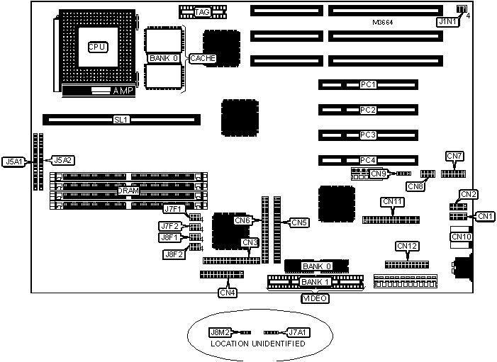
ADVANCED/AS
Processor | Pentium |
Processor Speed | 75/90/100/120/133/150/166/200MHz |
Chip Set | Intel |
Video Chip Set | ATI |
Maximum Onboard Memory | 128MB (EDO supported) |
Maximum Video Memory | 2MB |
Cache | 256/512KB |
BIOS | AMI |
Dimensions | 330mm x 218mm |
I/O Options | 32-bit PCI slots (4), floppy drive interface, green PC connector, IDE interfaces (2), parallel port, PS/2 mouse port, serial ports (2), VESA feature connector, riser slot, cache slot, IR connector, wave table connector, audio connector, CD-ROM connector |
NPU Options | None |
CONNECTIONS | |||
Purpose | Location | Purpose | Location |
Serial port 1 | CN1 | Turbo LED | J5A1 pins 1 & 2 |
Serial port 2 | CN2 | IDE interface LED | J5A1 pins 5 - 8 |
Floppy drive interface | CN3 | Power LED & keylock | J5A1 pins 10 - 15 |
Parallel port | CN4 | Reset switch | J5A1 pins 16 & 17 |
IDE interface 1 | CN5 | Green PC connector | J5A2 pins 1 & 2 |
IDE interface 2 | CN6 | IR connector | J5A2 pins 4 - 8 |
Video connector (optional) | CN7 | Chassis fan power | J5A2 pins 10 - 12 |
Wave table connector | CN8 | Speaker | J5A2 pins 14 - 17 |
CD-ROM interface | CN9 | Soft off/sleep | J7A1 |
PS/2 mouse port | CN10 | Soft power supply on | J8M2 |
Audio connector | CN11 | 32-bit PCI slots | PC1 - PC4 |
VESA feature connector | CN12 | Cache slot | SL1 |
USER CONFIGURABLE SETTINGS | |||
Function | Label | Position | |
Factory configured - do not alter (pins 1, 2, & 3 only) | J1N1 | N/A | |
» | Password normal operation | J7F1 | Pins 4 & 5 closed |
Password clear | J7F1 | Pins 5 & 6 closed | |
» | Setup access enabled | J7F2 | Pins 1 & 2 closed |
Setup access disabled | J7F2 | Pins 2 & 3 closed | |
» | CMOS memory normal operation | J7F2 | Pins 4 & 5 closed |
CMOS memory clear | J7F2 | Pins 5 & 6 closed | |
DRAM CONFIGURATION | ||
Size | Bank 0 | Bank 1 |
8MB | (2) 1M x 32 | None |
16MB | (2) 2M x 32 | None |
16MB | (2) 1M x 32 | (2) 1M x 32 |
24MB | (2) 2M x 32 | (2) 1M x 32 |
24MB | (2) 1M x 32 | (2) 2M x 32 |
32MB | (2) 4M x 32 | None |
32MB | (2) 2M x 32 | (2) 2M x 32 |
40MB | (2) 4M x 32 | (2) 1M x 32 |
40MB | (2) 1M x 32 | (2) 4M x 32 |
48MB | (2) 4M x 32 | (2) 2M x 32 |
48MB | (2) 2M x 32 | (2) 4M x 32 |
64MB | (2) 8M x 32 | None |
64MB | (2) 4M x 32 | (2) 4M x 32 |
72MB | (2) 8M x 32 | (2) 1M x 32 |
72MB | (2) 1M x 32 | (2) 8M x 32 |
80MB | (2) 8M x 32 | (2) 2M x 32 |
DRAM CONFIGURATION (CON’T) | ||
Size | Bank 0 | Bank 1 |
80MB | (2) 2M x 32 | (2) 8M x 32 |
96MB | (2) 8M x 32 | (2) 4M x 32 |
96MB | (2) 4M x 32 | (2) 8M x 32 |
128MB | (2) 8M x 32 | (2) 8M x 32 |
Note: Board accepts EDO memory. The location of banks 0 & 1 are unidentified. Board also accepts x 36 SIMMs. | ||
CACHE CONFIGURATION | |||
Size | Bank 0 | SL1 | TAG |
256KB | (2) 32K x 32 | None | Unidentified |
512KB | (2) 32K x 32 | 256KB module installed | Unidentified |
Note: The size of the TAG chip is unidentified. | |||
VIDEO MEMORY CONFIGURATION | ||
Size | Bank 0 | Bank 1 |
1MB | 1MB | None |
2MB | 1MB | (2) 256K x 16 |
Note: Bank 0 is factory installed and is not configurable. | ||
CPU SPEED SELECTION | |||||
CPU speed | Clock speed | Multiplier | J1N1 | J8F1 | J8F2 |
75MHz | 50MHz | 1.5x | 4 & 5 | 1 & 2, 5 & 6 | 1 & 2 |
90MHz | 60MHz | 1.5x | 4 & 5 | 1 & 2, 4 & 5 | 1 & 2 |
100MHz | 66MHz | 1.5x | 4 & 5 | 2 & 3, 5 & 6 | 1 & 2 |
120MHz | 60MHz | 2x | 4 & 5 | 1 & 2, 4 & 5 | 2 & 3 |
133MHz | 66MHz | 2x | 4 & 5 | 2 & 3, 5 & 6 | 2 & 3 |
150MHz | 60MHz | 2.5x | 5 & 6 | 1 & 2, 4 & 5 | 2 & 3 |
166MHz | 66MHz | 2.5x | 5 & 6 | 2 & 3, 5 & 6 | 2 & 3 |
200MHz | 66MHz | 3x | 5 & 6 | 2 & 3, 5 & 6 | 1 & 2 |
Note: Pins designated should be in the closed position. | |||||
CPU VOLTAGE SELECTION | |
Voltage | J8F2 |
3.3v - 3.3465v | Pins 4 & 5 closed |
3.465v - 3.63v | Pins 5 & 6 closed |
CPU ISA BUS CLOCK SELECTION | |||
Clock speed | Bus speed | J7F1 | |
50MHz | 8.33MHz | Pins 1 & 2 or 2 & 3 closed | |
| » | 60MHz | 7.5MHz | Pins 1 & 2 closed |
60MHz | 10MHz | Pins 2 & 3 closed | |
| » | 66MHz | 8.25MHz | Pins 1 & 2 closed |
66MHz | 11MHz | Pins 2 & 3 closed | |
My Books

