COMMUNIQUE 386 Motherboard Settings and Configuration
INTEGRATED WORKSTATIONS, INC.
COMMUNIQUE 386
Processor | 80386SX |
Processor Speed | 16/20MHz |
Chip Set | VLSI |
Max. Onboard DRAM | 32MB |
Cache | None |
BIOS | Quadtel |
Dimensions | 128mm x 365mm |
I/O Options | Keyboard & monochrome video port, network interface controller, parallel port, serial port (2) |
NPU Options | None |
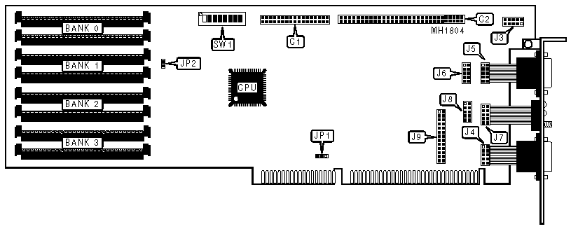
CONNECTIONS | |||
Purpose | Location | Purpose | Location |
Daughterboard | C1 & C2 | Reset switch & diagnostic LEDs | J7 |
Serial port 1 | J4 | LAN connection | J8 |
Keyboard & mono video port | J5 | Parallel port | J9 |
Serial port 2 | J6 | ||
USER CONFIGURABLE SETTINGS | |||
Function | Jumper | Position | |
» | Factory configured - do not alter | J3 | 7 & 8, 9 & 10 |
» | Monochrome controller and LPT1 control enabled | J3 | 1&2, 3&4, 5&6 closed |
Monochrome controller and LPT1 control disabled | J3 | 1&2, 3&4, 5&6 open | |
» | Host attention interrupt select IRQ10 at 0A Hex | JP1 | pins 1 & 2 closed |
Host attention interrupt select IRQ12 at 0A Hex | JP1 | pins 2 & 3 closed | |
» | Zero wait state enabled | JP2 | Closed |
Zero wait state disabled | JP2 | Open | |
Note:Pins designated should be in the closed position unless otherwise specified. | |||
DRAM CONFIGURATION | ||||
Size | Bank 0 | Bank 1 | Bank 2 | Bank 3 |
1MB | (2) 256K x 9 | (2) 256K x 9 | NONE | NONE |
1.5MB | (2) 256K x 9 | (2) 256K x 9 | (2) 256K x 9 | NONE |
2MB | (2) 256K x 9 | (2) 256K x 9 | (2) 256K x 9 | (2) 256K x 9 |
2MB | (2) 1M x 9 | NONE | NONE | NONE |
3MB | (2) 256K x 9 | (2) 256K x 9 | (2) 1M x 9 | NONE |
4MB | (2) 1M x 9 | (2) 1M x 9 | NONE | NONE |
4.5MB | (2) 1M x 9 | (2) 1M x 9 | (2) 256K x 9 | NONE |
5MB | (2) 256K x 9 | (2) 256K x 9 | (2) 1M x 9 | (2) 1M x 9 |
6MB | (2) 1M x 9 | (2) 1M x 9 | (2) 1M x 9 | NONE |
8MB | (2) 1M x 9 | (2) 1M x 9 | (2) 1M x 9 | (2) 1M x 9 |
8MB | (2) 4M x 9 | NONE | NONE | NONE |
9MB | (2) 256K x 9 | (2) 256K x 9 | (2) 4M x 9 | NONE |
10MB | (2) 1M x 9 | (2) 4M x 9 | NONE | NONE |
12MB | (2) 1M x 9 | (2) 1M x 9 | (2) 4M x 9 | NONE |
16MB | (2) 4M x 9 | (2) 4M x 9 | NONE | NONE |
16.5MB | (2) 4M x 9 | (2) 4M x 9 | (2) 256K x 9 | NONE |
17MB | (2) 256K x 9 | (2) 256K x 9 | (2) 4M x 9 | (2) 4M x 9 |
18MB | (2) 4M x 9 | (2) 4M x 9 | (2) 1M x 9 | NONE |
20MB | (2) 1M x 9 | (2) 1M x 9 | (2) 4M x 9 | (2) 4M x 9 |
24MB | (2) 4M x 9 | (2) 4M x 9 | (2) 4M x 9 | NONE |
32MB | (2) 4M x 9 | (2) 4M x 9 | (2) 4M x 9 | (2) 4M x 9 |
MEMORY BASE ADDRESS | |||
Address | SW1/switch 7 | SW1/switch 8 | |
| » | DC000h | Off | Off |
CC000h | On | Off | |
FCC000h | On | On | |
FDC000h | Off | On | |
NODE ID ADDRESS | ||||||
Node | SW1/1 | SW1/2 | SW1/3 | SW1/4 | SW1/5 | SW1/6 |
0 | Off | Off | Off | Off | Off | Off |
1 | On | Off | Off | Off | Off | Off |
2 | Off | On | Off | Off | Off | Off |
3 | On | On | Off | Off | Off | Off |
4 | Off | Off | On | Off | Off | Off |
59 | On | On | Off | On | On | On |
60 | Off | Off | On | On | On | On |
61 | On | Off | On | On | On | On |
62 | Off | On | On | On | On | On |
63 | On | On | On | On | On | On |
Note:A total of 63 node address settings are available. The switches are a binary representation of the decimal node addresses, and have the following decimal values: 1=1, 2=2, 3=4, 4=8, 5=16, 6=32. Switches in the off position maintain a zero value. Sum total the switches in the on position to obtain the correct node address. Node 0 is a non-valid address. | ||||||
My Books

