LX400A/P VLB Motherboard Settings and Configuration
BCM ADVANCED RESEARCH, INC.
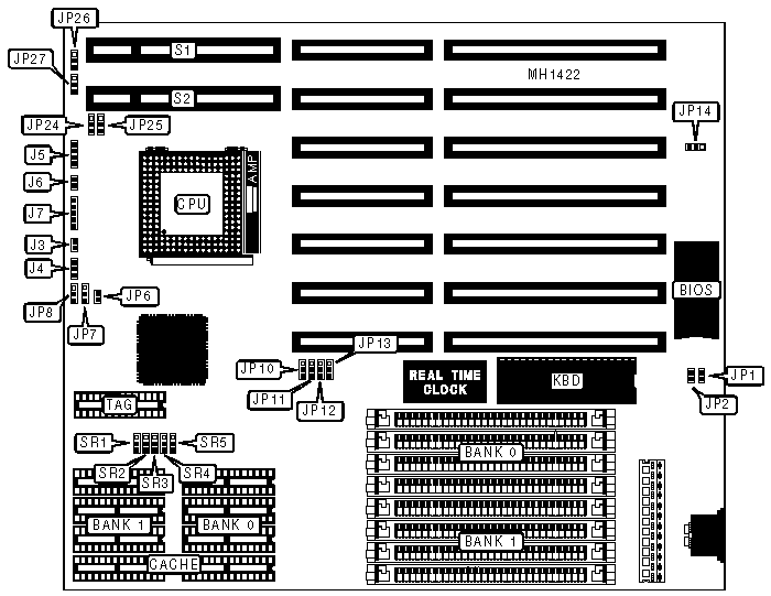
LX400A/P VLB
Processor | 80486SX/80487SX/80486DX/80486DX2 |
Processor Speed | 20/25/33/50(internal)/50/66(internal) |
Chip Set | SIS |
Max. Onboard DRAM | 32MB |
SRAM Cache | 64/128/256KB |
BIOS | AMI |
Dimensions | 254mm x 218mm |
I/O Options | 32-bit VESA local bus slot (2) |
NPU Options | None |
CONNECTIONS | |||
Purpose | Location | Purpose | Location |
Turbo LED | J3 | Power LED & keylock | J7 |
Turbo switch | J4 | 32-bit VESA local bus slot | S1 |
Speaker | J5 | 32-bit VESA local bus slot | S2 |
Reset switch | J6 |
|
|
32-BIT VESA LOCAL BUS SLOT CONFIGURATION | ||||
CPU Speed | JP24 | JP25 | JP26 | JP27 |
<=33MHz | pins 1 & 2 closed | pins 1 & 2 closed | pins 1 & 2 closed | pins 1 & 2 closed |
> 33MHz | pins 2 & 3 closed | pins 2 & 3 closed | pins 2 & 3 closed | pins 2 & 3 closed |
USER CONFIGURABLE SETTINGS | |||
Function | Jumper/Switch | Position | |
» | Factory configured - do not alter | JP1 | open |
» | Monitor type select color | JP2 | closed |
| Monitor type select monochrome | JP2 | open |
» | Power good signal detect from power supply | JP14 | pins 1 & 2 closed |
| Power good signal detect from board | JP14 | pins 2 & 3 closed |
SRAM CONFIGURATION | |||
Size | Cache | Location | TAG |
64KB | (8) 8K x 8 | Banks 0 & 1 | (1) 8K x 8 |
128KB | (4) 32K x 8 | Bank 0 | (1) 8K x 8 |
256KB | (8) 32K x 8 | Banks 0 & 1 | (2) 32K x 8 |
SRAM JUMPER CONFIGURATION | |||||
Size | SR1 | SR2 | SR3 | SR4 | SR5 |
64KB | pins 2 & 3 | pins 2 & 3 | pins 1 & 2 | pins 1 & 2 | pins 1 & 2 |
128KB | pins 1 & 2 | pins 1 & 2 | pins 2 & 3 | pins 2 & 3 | pins 1 & 2 |
256KB | pins 2 & 3 | pins 2 & 3 | pins 2 & 3 | pins 2 & 3 | pins 2 & 3 |
Note:Pins designated should be in the closed position. | |||||
CPU SPEED SELECTION | ||||
Speed | JP10 | JP11 | JP12 | JP13 |
20MHz | pins 2 & 3 | pins 2 & 3 | pins 2 & 3 | pins 2 & 3 |
25MHz/50(internal) | pins 2 & 3 | pins 2 & 3 | pins 1 & 2 | pins 1 & 2 |
33MHz/66(internal) | pins 1 & 2 | pins 2 & 3 | pins 1 & 2 | pins 1 & 2 |
50MHz | pins 1 & 2 | pins 1 & 2 | pins 1 & 2 | pins 1 & 2 |
Note:Pins designated should be in the closed position. | ||||
CPU TYPE CONFIGURATION | |||
CPU type | JP6 | JP7 | JP8 |
80486SX | open | open | pins 2 & 3 closed |
80487SX | closed | pins 2 & 3 closed | pins 1 & 2 closed |
80486DX/DX2 | closed | pins 1 & 2 closed | pins 1 & 2 closed |
DRAM CONFIGURATION | ||
Size | Bank 0 | Bank 1 |
1MB | (4) 256K x 9 | NONE |
2MB | (4) 256K x 9 | (4) 256K x 9 |
4MB | (4) 1M x 9 | NONE |
8MB | (4) 1M x 9 | (4) 1M x 9 |
16MB | (4) 4M x 9 | NONE |
20MB | (4) 1M x 9 | (4) 4M x 9 |
32MB | (4) 4M x 9 | (4) 4M x 9 |
My Books

