ACERPOWER 486 (V20 PROJECT) Motherboard Settings and Configuration
ACER, INC.
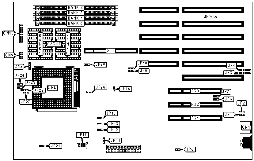
ACERPOWER 486 (V20 PROJECT)
Processor | 80486SX/80486SX2/80486DX/80486DX2/80486DX4/Pentium Overdrive |
Processor Speed | 25/33/50(internal)/66(internal)/75(internal)/100(internal)MHz |
Chip Set | Unidentified |
Max. Onboard DRAM | 64MB |
Cache | 128/256/512KB |
BIOS | Acer |
Dimensions | 330mm x 218mm |
I/O Options | 32-bit VESA local bus slot, 32-bit PCI slots (3), green PC connector, PS/2 mouse port |
NPU Options | None |
CONNECTIONS | |||
Purpose | Location | Purpose | Location |
PS/2 mouse port | CN1 | 32-bit VESA local bus slot | SL1 |
32-bit PCI slots | PC1 - PC3 | ||
USER CONFIGURABLE SETTINGS | |||
Function | Jumper | Position | |
» | Factory configured - do not alter | CN8 | N/A |
» | Factory configured - do not alter | CN9 | N/A |
» | Factory configured - do not alter | CN10 | N/A |
» | Password enabled | JP1 | pins 1 & 2 closed |
Password disabled | JP1 | pins 2 & 3 closed | |
» | BIOS type select Acer | JP2 | pins 1 & 2 closed |
BIOS type select OEM | JP2 | pins 2 & 3 closed | |
» | Factory configured - do not alter | JP3 | pins 3 & 4 closed |
» | Factory configured - do not alter | JP4 | pins 1 & 2, 3 & 4, 5 & 6 closed |
Factory configured - do not alter | JP6 | pins 2 & 3 closed | |
» | Factory configured - do not alter | JP7 | pins 2 & 3 closed |
» | M5115 enabled | JP8 | pins 1 & 2 closed |
M5115 disabled | JP8 | pins 2 & 3 closed | |
» | Factory configured - do not alter | JP10 | pins 1 & 2 closed |
» | Local bus IDE I/O address select 0FXH | JP11 | pins 1 & 2 closed |
Local bus IDE I/O address select 07XH | JP11 | pins 2 & 3 closed | |
» | Local bus IDE interface enabled | JP12 | pins 2 & 3 closed |
Local bus IDE interface disabled | JP12 | pins 1 & 2 closed | |
» | Reset button enabled | JP23 | pins 1 & 2 closed |
Reset button disabled | JP23 | pins 2 & 3 closed | |
» | Power saving feature disabled | JP24 | pins 2 & 3 closed |
Power saving feature enabled | JP24 | pins 1 & 2 closed | |
DRAM CONFIGURATION | ||||
Size | Bank 0 | Bank 1 | Bank 2 | Bank 3 |
4MB | (1) 1M x 36 | NONE | NONE | NONE |
8MB | (1) 1M x 36 | (1) 1M x 36 | NONE | NONE |
12MB | (1) 1M x 36 | (1) 1M x 36 | (1) 1M x 36 | NONE |
12MB | (1) 1M x 36 | NONE | (1) 2M x 36 | NONE |
16MB | (1) 1M x 36 | (1) 1M x 36 | (1) 1M x 36 | (1) 1M x 36 |
16MB | (1) 2M x 36 | NONE | (1) 2M x 36 | NONE |
16MB | (1) 4M x 36 | NONE | NONE | NONE |
32MB | (1) 4M x 36 | (1) 4M x 36 | NONE | NONE |
48MB | (1) 4M x 36 | (1) 4M x 36 | (1) 4M x 36 | NONE |
64MB | (1) 4M x 36 | (1) 4M x 36 | (1) 4M x 36 | (1) 4M x 36 |
CACHE CONFIGURATION | |||
Size | Bank 0 | Bank 1 | TAG |
128KB | (4) 32K x 8 | NONE | (1) 32K x 8 |
256KB | (4) 32K x 8 | (4) 32K x 8 | (1) 32K x 8 |
512KB | NONE | (4) 128K x 8 | (1) 32K x 8 |
Note: The location of the TAG is unidentified. | |||
CACHE JUMPER CONFIGURATION | |||
Size | J13 | J15 | J16 |
128KB | pins 2 & 3 closed | pins 2 & 3 closed | pins 1 & 2 closed |
256KB | pins 2 & 3 closed | pins 1 & 2 closed | pins 2 & 3 closed |
512KB | pins 1 & 2 closed | pins 1 & 2 closed | pins 1 & 2 closed |
CPU TYPE CONFIGURATION | ||
Type | JP9 | JP20 |
80486SX | pins 2 & 3 closed | pins 1 & 2 closed |
80486SX2 | pins 2 & 3 closed | pins 1 & 2 closed |
80486DX | pins 2 & 3 closed | pins 1 & 2 closed |
80486DX2 | pins 2 & 3 closed | pins 1 & 2 closed |
80486DX4 | pins 2 & 3 closed | pins 1 & 2 closed |
Pentium Overdrive | pins 1 & 2 closed | pins 2 & 3 closed |
CPU TYPE CONFIGURATION | ||
Type | JP26 | JP27 |
Intel | pins 1 & 2 closed | pins 1 & 2 closed |
AMD | pins 2 & 3 closed | pins 2 & 3 closed |
CPU SPEED CONFIGURATION | ||
Speed | JP17 | JP21 |
25MHz | pins 1 & 5 closed | pins 2 & 3 closed |
33MHz | pins 2 & 6 closed | pins 2 & 3 closed |
50iMHz | pins 1 & 5 closed | pins 2 & 3 closed |
66iMHz | pins 2 & 6 closed | pins 2 & 3 closed |
75iMHz | pins 1 & 5 closed | pins 2 & 3 closed |
100iMHz | pins 2 & 6 closed | pins 2 & 3 closed |
CPU SPEED CONFIGURATION (80486DX4 ONLY) | |
Speed | JP22 |
2.0x | pins 1 & 2 closed |
2.5x | pins 2 & 3 closed |
3.0x | pins 3 & 4 closed |
My Books

