ADVANCE A/D-D/A DIGITAL I/O CARD IO card Settings and Configuration
DECISION COMPUTER INTERNATIONAL CO., LTD.
ADVANCE A/D-D/A DIGITAL I/O CARD
Card Type | Data acquisition |
Chipset | Signal Processing Technologies HADC674Z |
I/O Options | Analog/digital I/O |
Data Bus | 8-bit ISA |
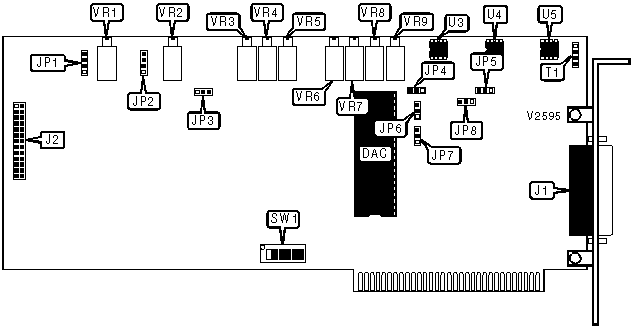
CONNECTIONS | |||
Function | Label | Function | Label |
Analog/digital I/O (see pinout below) | J1 | Analog-to-digital negative bipolar offset voltage | VR3 |
Analog/digital I/O (see pinout below) | J2 | Analog-to-digital positive bipolar offset voltage | VR4 |
Unidentified | T1 | Analog-to-digital unipolar offset voltage | VR5 |
Unidentified | U3 | Buffer gain voltage | VR6 |
Unidentified | U4 | U3 offset voltage | VR7 |
Unidentified | U5 | U4 offset voltage | VR8 |
Digital-to-analog channel 1 voltage | VR1 | U5 offset voltage | VR9 |
Digital-to-analog channel 2 voltage | VR2 | ||
J1 PINOUT (SINGLE-ENDED) | |||
Function | Pin | Function | Pin |
+12V DC power | 1 | -12V DC power | 14 |
Digital-to-analog channel 2 output | 2 | Digital-to-analog channel 1 output | 15 |
Ground | 3 | Analog-to-digital channel 15 | 16 |
Analog-to-digital channel 14 | 4 | Analog-to-digital channel 13 | 17 |
Analog-to-digital channel 12 | 5 | Analog-to-digital channel 11 | 18 |
Analog-to-digital channel 10 | 6 | Analog-to-digital channel 9 | 19 |
Analog-to-digital channel 8 | 7 | Analog-to-digital channel 7 | 20 |
Analog-to-digital channel 6 | 8 | Analog-to-digital channel 5 | 21 |
Analog-to-digital channel 4 | 9 | Analog-to-digital channel 3 | 22 |
Analog-to-digital channel 2 | 10 | Analog-to-digital channel 1 | 23 |
Analog-to-digital channel 0 | 11 | Ground | 24 |
Ground | 12 | -5V DC power | 25 |
+5V DC power | 13 | ||
J1 PINOUT (DIFFERENTIAL) | |||
Function | Pin | Function | Pin |
+12V DC power | 1 | -12V DC power | 14 |
Digital-to-analog channel 2 output | 2 | Digital-to-analog channel 1 output | 15 |
Ground | 3 | Analog-to-digital negative channel 7 | 16 |
Analog-to-digital positive channel 7 | 4 | Analog-to-digital negative channel 6 | 17 |
Analog-to-digital positive channel 6 | 5 | Analog-to-digital negative channel 5 | 18 |
Analog-to-digital positive channel 5 | 6 | Analog-to-digital negative channel 4 | 19 |
Analog-to-digital positive channel 4 | 7 | Analog-to-digital negative channel 3 | 20 |
Analog-to-digital positive channel 3 | 8 | Analog-to-digital negative channel 2 | 21 |
Analog-to-digital positive channel 2 | 9 | Analog-to-digital negative channel 1 | 22 |
Analog-to-digital positive channel 1 | 10 | Analog-to-digital negative channel 0 | 23 |
Analog-to-digital positive channel 0 | 11 | Ground | 24 |
Ground | 12 | -5V DC power | 25 |
+5V DC power | 13 | ||
J2 PINOUT | |||
Function | Pin | Function | Pin |
+12V DC power | 1 | Digital channel 2 bit 1 | 14 |
Ground | 2 | Digital channel 2 bit 2 | 15 |
+12V DC power | 3 | Digital channel 2 bit 3 | 16 |
Ground | 4 | Digital channel 2 bit 4 | 17 |
Digital channel 1 bit 0 | 5 | Digital channel 2 bit 5 | 18 |
Digital channel 1 bit 1 | 6 | Digital channel 2 bit 6 | 19 |
Digital channel 1 bit 2 | 7 | Digital channel 2 bit 7 | 20 |
Digital channel 1 bit 3 | 8 | Chip Select 1 | 21 |
Digital channel 1 bit 4 | 9 | Chip Select 2 | 22 |
Digital channel 1 bit 5 | 10 | +5V DC power | 23 |
Digital channel 1 bit 6 | 11 | Ground | 24 |
Digital channel 1 bit 7 | 12 | -12V DC power | 25 |
Digital channel 2 bit 0 | 13 | Ground | 26 |
ANALOG-TO-DIGITAL VOLTAGE RANGE | ||||
Setting | JP4 | JP6 | JP7 | |
0V to 10V | Pins 1 & 2 closed | Pins 1 & 2 closed | Pins 2 & 3 closed | |
0V to 20V | Pins 1 & 2 closed | Pins 2 & 3 closed | Pins 2 & 3 closed | |
| » | -10V to 10V | Pins 1 & 2 closed | Pins 1 & 2 closed | Pins 1 & 2 closed |
-20V to 20V | Pins 1 & 2 closed | Pins 2 & 3 closed | Pins 1 & 2 closed | |
Set by VR3 - VR5 | Pins 2 & 3 closed | N/A | N/A | |
DIGITAL-TO-ANALOG CHANNEL 1 VOLTAGE | |||
Setting | JP1 | JP4 | |
0V to 10V | Pins 3 & 4 closed | Pins 1 & 2 closed | |
| » | -10V to 10V | Pins 1 & 2 closed | Pins 1 & 2 closed |
Set by VR1 | N/A | Pins 2 & 3 closed | |
DIGITAL-TO-ANALOG CHANNEL 2 VOLTAGE | |||
Setting | JP2 | JP4 | |
0V to 10V | Pins 3 & 4 closed | Pins 1 & 2 closed | |
| » | -10V to 10V | Pins 1 & 2 closed | Pins 1 & 2 closed |
Set by VR2 | N/A | Pins 2 & 3 closed | |
SINGLE-ENDED/DIFFERENTIAL MODE | |||
Setting | JP3 | JP5 | JP8 |
Single-ended | Pins 1 & 2 closed | Pins 1 & 2 closed | Pins 2 & 3 closed |
Differential | Pins 2 & 3 closed | Pins 2 & 3 closed | Pins 3 & 4 closed |
BASE I/O ADDRESS | ||||||
Setting | SW1/1 | SW1/2 | SW1/3 | SW1/4 | SW1/5 | SW1/6 |
000h | On | On | On | On | On | On |
010h | On | On | On | On | On | Off |
020h | On | On | On | On | Off | On |
030h | On | On | On | On | Off | Off |
040h | On | On | On | Off | On | On |
3B0h | Off | Off | Off | On | Off | Off |
3C0h | Off | Off | Off | Off | On | On |
3D0h | Off | Off | Off | Off | On | Off |
3E0h | Off | Off | Off | Off | Off | On |
3F0h | Off | Off | Off | Off | Off | Off |
Note:A total of 64 base address settings are available. The switches are a binary representation of the decimal memory addresses. SW1/1 is the Most Significant Bit and switch SW1/6 is the Least Significant Bit. The switches have the following decimal values: SW1/1=512, SW1/2=256, SW1/3=128, SW1/4=64, SW1/5=32, SW1/6=16. Turn off the switches and add the values of the switches that are off to obtain the correct address. (Off=1, On=0) | ||||||
My Books

