8 CHANNEL RELAY OUTPUT/PHOTO-ISOLATOR IO card Settings and Configuration
DECISION COMPUTER INTERNATIONAL CO., LTD.
8 CHANNEL RELAY OUTPUT/PHOTO-ISOLATOR
Card Type | Data acquisition |
Chip Set | NEC 8255 |
I/O Options | Opto-isolated input and relay control output port |
Data Bus | 8-bit ISA |
CONNECTIONS | |
Function | Label |
Opto-isolated input and relay control output port | CN1 |
CN1 PINOUT | |||
Function | Pin | Function | Pin |
Channel 1 relay open | 1 | Channel 4 relay open | 20 |
Channel 1 relay common | 2 | Channel 4 relay common | 21 |
Channel 1 relay closed | 3 | Channel 4 relay closed | 22 |
Channel 2 relay open | 4 | Channel 5 relay open | 23 |
Channel 2 relay common | 5 | Channel 5 relay common | 24 |
Channel 2 relay closed | 6 | Channel 6 relay open | 25 |
Channel 3 relay open | 7 | Channel 6 relay common | 26 |
Channel 3 relay common | 8 | Channel 7 relay open | 27 |
Channel 3 relay closed | 9 | Channel 7 relay common | 28 |
Channel 8 relay open | 10 | Ground | 29 |
Channel 8 relay common | 11 | Channel 1 negative | 30 |
Channel 1 positive | 12 | Channel 2 negative | 31 |
Channel 2 positive | 13 | Channel 3 negative | 32 |
Channel 3 positive | 14 | Channel 4 negative | 33 |
Channel 4 positive | 15 | Channel 5 negative | 34 |
Channel 5 positive | 16 | Channel 6 negative | 35 |
Channel 6 positive | 17 | Channel 7 negative | 36 |
Channel 7 positive | 18 | Channel 8 negative | 37 |
Channel 8 positive | 19 | ||
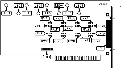
OPTO-ISOLATION OPTIONS | ||
Setting | JPxA | JPxB |
Differential signals (+ and -) | Pins 1 & 2 closed | Pins 2 & 3 closed |
Single-ended signals (+ and GND) | Pins 1 & 2 closed | Pins 1 & 2 closed |
Single-ended signals, TTL levels | Pins 2 & 3 closed | N/A |
Note:The exact locations of JP1A through JP8A and JP1B through JP8B are unidentified. JP1A and JP1B control the opto-isolation functions of channel 1. The settings for JP2A through JP8A and JP2B through JP8B are identical, controlling channels 2 through 8 respectively. | ||
BASE I/O ADDRESS | |||||||||
Setting | SW1/1 | SW1/2 | SW1/3 | SW1/4 | SW1/5 | SW1/6 | SW1/7 | SW1/8 | |
000h | On | On | On | On | On | On | On | On | |
004h | On | On | On | On | On | On | On | Off | |
008h | On | On | On | On | On | On | Off | On | |
010h | On | On | On | On | On | Off | On | On | |
014h | On | On | On | On | On | Off | On | Off | |
| » | 2A8h | Off | On | Off | On | Off | On | Off | On |
3ECh | Off | Off | Off | Off | Off | On | Off | Off | |
3F0h | Off | Off | Off | Off | Off | Off | On | On | |
3F4h | Off | Off | Off | Off | Off | Off | On | Off | |
3F8h | Off | Off | Off | Off | Off | Off | Off | On | |
3FCh | Off | Off | Off | Off | Off | Off | Off | Off | |
Note: Over 255 base address settings are available. The switches are a binary representation of the decimal memory addresses. SW1/1 is the Most Significant Bit and switch SW1/8 is the Least Significant Bit. The switches have the following decimal values: SW1/1=512, SW1/2=256, SW1/3=128, SW1/4=64, SW1/5=32, SW1/6=16, SW1/7=8, SW1/8=4. Turn off the switches and add the values of the switches that are off to 512 to obtain the correct memory address. (Off=1, On=0) | |||||||||
DIAGNOSTIC LED(S) |
The functions of the LEDs are unidentified. |
My Books

