8 CHANNEL 12/14-BIT D/A CARD IO card Settings and Configuration
DECISION COMPUTER INTERNATIONAL CO., LTD.
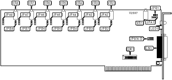
8 CHANNEL 12/14-BIT D/A CARD
Card Type | Data acquisition |
Chipset | Signal Processing Technologies |
I/O Options | Analog/digital I/O |
Data Bus | 8-bit ISA |
CONNECTIONS | |||
Function | Label | Function | Label |
Analog/digital I/O (see pinout below) | CN1 | Channel 5 reference voltage | VR5 |
Channel 1 reference voltage | VR1 | Channel 6 reference voltage | VR6 |
Channel 2 reference voltage | VR2 | Channel 7 reference voltage | VR7 |
Channel 3 reference voltage | VR3 | Channel 8 reference voltage | VR8 |
Channel 4 reference voltage | VR4 | ||
J1 PINOUT | |||
Function | Pin | Function | Pin |
+12V DC power | 1 | -12V DC power | 14 |
Not used | 2 | Not used | 15 |
Ground | 3 | Analog-to-digital channel 8 current | 16 |
Analog-to-digital channel 8 voltage | 4 | Analog-to-digital channel 7 current | 17 |
Analog-to-digital channel 7 voltage | 5 | Analog-to-digital channel 6 current | 18 |
Analog-to-digital channel 6 voltage | 6 | Analog-to-digital channel 5 current | 19 |
Analog-to-digital channel 5 voltage | 7 | Analog-to-digital channel 4 current | 20 |
Analog-to-digital channel 4 voltage | 8 | Analog-to-digital channel 3 current | 21 |
Analog-to-digital channel 3 voltage | 9 | Analog-to-digital channel 2 current | 22 |
Analog-to-digital channel 2 voltage | 10 | Analog-to-digital channel 1 current | 23 |
Analog-to-digital channel 1 voltage | 11 | Ground | 24 |
Ground | 12 | -5V DC power | 25 |
+5V DC power | 13 | ||
USER CONFIGURABLE SETTINGS | |||
Setting | Label | Position | |
| » | Factory configured - do not alter | SW1/7 | Off |
| » | Factory configured - do not alter | SW1/8 | Off |
| » | Channel 1 voltage is 0V to 9V | JPA1 | Pins 3 & 4 closed |
Channel 1 voltage is -9V to 9V | JPA1 | Pins 1 & 2 closed | |
| » | Channel 2 voltage is 0V to 9V | JPA2 | Pins 3 & 4 closed |
Channel 2 voltage is -9V to 9V | JPA2 | Pins 1 & 2 closed | |
| » | Channel 3 voltage is 0V to 9V | JPA3 | Pins 3 & 4 closed |
Channel 3 voltage is -9V to 9V | JPA3 | Pins 1 & 2 closed | |
| » | Channel 4 voltage is 0V to 9V | JPA4 | Pins 3 & 4 closed |
Channel 4 voltage is -9V to 9V | JPA4 | Pins 1 & 2 closed | |
| » | Channel 5 voltage is 0V to 9V | JPA5 | Pins 3 & 4 closed |
Channel 5 voltage is -9V to 9V | JPA5 | Pins 1 & 2 closed | |
| » | Channel 6 voltage is 0V to 9V | JPA6 | Pins 3 & 4 closed |
Channel 6 voltage is -9V to 9V | JPA6 | Pins 1 & 2 closed | |
| » | Channel 7 voltage is 0V to 9V | JPA7 | Pins 3 & 4 closed |
Channel 7 voltage is -9V to 9V | JPA7 | Pins 1 & 2 closed | |
| » | Channel 8 voltage is 0V to 9V | JPA8 | Pins 3 & 4 closed |
Channel 8 voltage is -9V to 9V | JPA8 | Pins 1 & 2 closed | |
| » | Factory configured - do not alter | JPB1 | Open |
| » | Factory configured - do not alter | JPB2 | Open |
| » | Factory configured - do not alter | JPB3 | Open |
| » | Factory configured - do not alter | JPB4 | Open |
| » | Factory configured - do not alter | JPB5 | Open |
| » | Factory configured - do not alter | JPB6 | Open |
| » | Factory configured - do not alter | JPB7 | Open |
| » | Factory configured - do not alter | JPB8 | Open |
BASE I/O ADDRESS | |||||||
Setting | SW1/1 | SW1/2 | SW1/3 | SW1/4 | SW1/5 | SW1/6 | |
000h | On | On | On | On | On | On | |
010h | On | On | On | On | On | Off | |
020h | On | On | On | On | Off | On | |
030h | On | On | On | On | Off | Off | |
040h | On | On | On | Off | On | On | |
| » | 2B0h | Off | On | Off | On | Off | Off |
3B0h | Off | Off | Off | On | Off | Off | |
3C0h | Off | Off | Off | Off | On | On | |
3D0h | Off | Off | Off | Off | On | Off | |
3E0h | Off | Off | Off | Off | Off | On | |
3F0h | Off | Off | Off | Off | Off | Off | |
Note: A total of 64 base address settings are available. The switches are a binary representation of the decimal memory addresses. SW1/1 is the Most Significant Bit and switch SW1/6 is the Least Significant Bit. The switches have the following decimal values: SW1/1=512, SW1/2=256, SW1/3=128, SW1/4=64, SW1/5=32, SW1/6=16. Turn off the switches and add the values of the switches that are off to obtain the correct memory address. (Off=1, On=0) | |||||||
WAIT STATES | ||||
Setting | JP9/A | JP9/B | JP9/C | JP9/D |
0 | Closed | Open | Open | Open |
1 | Open | Closed | Open | Open |
2 | Open | Open | Closed | Open |
3 | Open | Open | Open | Closed |
DIAGNOSTIC LED(S) |
The function of the LED is unidentified. |
My Books

