ASYNCHRONOUS SNA ADAPTER IO card Settings and Configuration
ATTACHMATE CORPORATION
ASYNCHRONOUS SNA ADAPTER
Card Type | Serial card |
Chip Set | Unidentified |
Data Bus | 8-bit ISA |
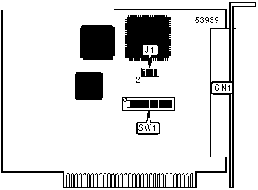
CONNECTIONS | |
Function | Label |
Connector | CN1 |
BASE I/O ADDRESS SELECTION | ||||||
Setting | SW1/6 | SW1/7 | SW1/8 | SW1/9 | SW1/10 | |
208 | On | On | On | On | On | |
218 | On | On | On | On | Off | |
228 | On | On | On | Off | On | |
238 | On | On | On | Off | Off | |
248 | On | On | Off | On | On | |
| » | 338 | Off | On | On | Off | Off |
3B8 | Off | Off | On | Off | Off | |
3C8 | Off | Off | Off | On | On | |
3D8 | Off | Off | Off | On | Off | |
3E8 | Off | Off | Off | Off | On | |
3F8 | Off | Off | Off | Off | Off | |
Note: A total of 32 base address settings are available. The switches are a binary representation of the decimal memory addresses. SW1/10 is the Most Significant Bit and switch SW1/5 is the Least Significant Bit. The switches have the following decimal values: SW1/10=256, SW1/9=128, SW8/10=64, SW1/7=32, SW1/6=16. Turn off the switches and add the values of the switches to 512 and convert to hexadecimal to obtain the correct memory address. (Off=1, On=0) | ||||||
MEMORY ADDRESS SELECTION | ||||||
Setting | SW1/1 | SW1/2 | SW1/3 | SW1/4 | SW1/5 | |
83FFF | On | On | On | On | On | |
87FFF | On | On | On | On | Off | |
8BFFF | On | On | On | Off | On | |
8FFFF | On | On | On | Off | Off | |
93FFF | On | On | Off | On | Off | |
| » | D3FFF | Off | On | Off | On | On |
EFFFF | Off | Off | On | Off | Off | |
F3FFF | Off | Off | Off | On | On | |
F7FFF | Off | Off | Off | On | Off | |
FBFFF | Off | Off | Off | Off | On | |
FFFFF | Off | Off | Off | Off | Off | |
Note: A total of 32 base address settings are available. The switches are a binary representation of the decimal memory addresses. SW1/5 is the Most Significant Bit and switch SW1/1 is the Least Significant Bit. The switches have the following decimal values: SW1/5=262144, SW1/4=131072, SW3/10=65536, SW1/2=32768, SW1/1=16384. Turn off the switches and add the values of the switches to 540671 and convert to hexadecimal to obtain the correct memory address. (Off=1, On=0) | ||||||
SERIAL PORT INTERRUPT SELECTION | |
IRQ | JP3 |
IRQ2 | Pins 1 & 2 closed |
IRQ3 | Pins 3 & 4 closed |
IRQ4 | Pins 5 & 6 closed |
IRQ5 | Pins 7 & 8 closed |

My Books