TVGA 8902/4/8-DRAM video card Settings and Configuration
UNIDENTIFIED
TVGA 8902/4/8-DRAM
Card Type | Video Card |
Video Chip Set | Unidentified |
Maximum Video Memory | 1MB DRAM |
Video Types Supported | VGA |
Highest Resolution Supported | 1024 x 768 |
Data Bus | 16-bit ISA |
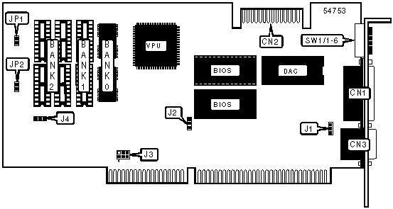
CONNECTIONS | |||
Function | Label | Function | Label |
15-pin analog video port | CN1 | 9-pin TTL Port | CN3 |
Feature connector (VGA/VESA) | CN2 |
|
|
USER CONFIGURABLE SETTINGS | |||
Function | Label | Position | |
» | Unidentified | SW1/4 | On |
BUS SIZE DETECTION | ||
Setting | J2 | |
» | Autodetect | Pins 2 & 3 Closed |
| Standard Interface | Pins 1 & 2 Closed |
Note: Orientation of J2 may vary. Check pin numbers on card. | ||
BUS SIZE SELECTION | ||
Setting | SW1/6 | |
» | 16-bit | Off |
| 8-bit | On |
SCAN RATE SELECTION | ||
Rate | SW1/3 | |
» | Less than 48Mhz | On |
| 48-49Mhz | Off |
MONITOR SELECT | ||
Setting | SW1/1 | SW1/2 |
VGA | On | On |
EGA | Off | On |
CGA | On | Off |
MDA/Hercules | Off | Off |
Note: SW1/1 & 2 affects 9-pin TTL connection. Not present on all cards. | ||
INTERRUPT | ||
IRQ 9 | J1 | |
» | Disabled | Pins 2 & 3 Closed |
| Enabled | Pins 1 & 2 Closed |
ADDRESS DECODE | ||
Setting | SW1/5 | |
» | Fast address decode | Off |
| Slow address decode | On |
DRAM CONFIGURATION | |||
Size | Bank 0 | Bank 1 | Bank 2 |
256KB | (2) 128KB x 4 | None | None |
512KB | (2) 128KB x 4 | (2) 128KB x 4 | None |
1MB | (2) 128KB x 4 | (2) 128KB x 4 | (4) 128KB x 4 |
VIDEO MEMORY JUMPER CONFIGURATION | |||
Size | JP1 | JP2 | J3 |
256KB | Open | Closed | Pins 1 & 2, 4 & 5 closed |
512KB | Open | Closed | Pins 1 & 4, 2 & 5 closed |
1MB | Closed | Open | Pins 2 &3, 5 & 6 closed |
Note: JP1 &2 are jumper blocks, number of pins unidentified. Not present on all cards. Orientation of J3 may vary. | |||
CLOCK SPEED | ||
Setting | J4 | |
» | 40Mhz(2 DRAM) | Pins 2 & 3 closed |
| 48Mhz(4/8 DRAM) | Pins 1 & 2 closed |
Note: Exact location of J4 unidentified. Not present on all cards | ||


My Books